Display
PRELIMINARY INFORMATION
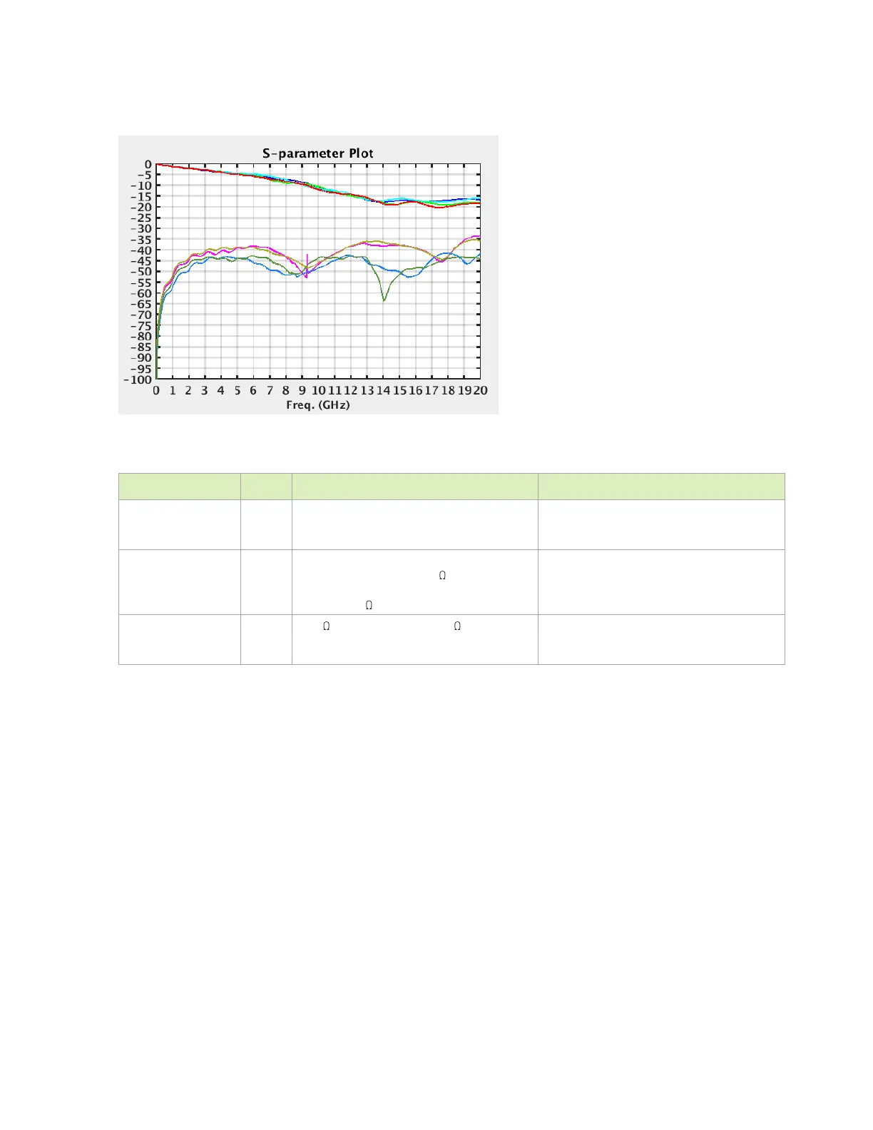
Jetson Orin NX Series and Jetson Orin Nano Series DG-10931-001_v1.1 | 51
Figure 9-5. S-Parameter Up to HBR3
Table 9-4. eDP and DP Signal Connections
Series 0.1uF capacitors and ESD to GND on
all.
eDP/DP Differential CLK/Data Lanes:
Connect to matching pins on display
connector.
Series 0.1uF capacitors DP1_AUX_CH_P
pulled to GND through 100k resistor.
DP1_AUX_CH_N pulled to VDD_3V3_DP
through 100k resistor.
eDP/DP: Auxiliary Channels: Connect to
AUX_CH-/+ on display connector.
100k series resistor and 100k resistor to
GND then Level shifter (non-inverting)
between connector and module pin.
eDP/DP: Hot Plug Detect: Connect to HPD
pin on display connector through level shifter.
 Loading...


