Display
PRELIMINARY INFORMATION
Jetson Orin NX Series and Jetson Orin Nano Series DG-10931-001_v1.1 | 50
Voiding
RBR/HBR
HBR2/HBR3
No requirement
Voiding required
HBR2: Voiding the plane directly under the
pad ~0.1mm larger than the pad size is
recommended.
Serpentine (See USB 3.2 Guidelines)
Voiding
RBR/HBR
HBR2/HBR3
No requirement
Voiding required
HBR2: Standard DP Connector: Voiding
requirement is stack-up dependent. For
typical stack-ups, voiding on the layer under
the connector pad is required to be 5.7 mil
larger than the connector pad.
Keep critical PCIe traces away from other signal traces or unrelated power traces/areas or power supply components
Notes:
1. For eDP and DP, the specification puts a higher priority on the trace loss characteristic than on the impedance. However, before
selecting 85 -up, material and trace dimension can achieve the
needed low loss characteristic.
2. The average of the differential signals is used for length and delay matching.
3. Do not perform length and delay matching within breakout region. Recommend doing trace length and delay matching to <1ps
before vias or any discontinuity to minimize common mode conversion.
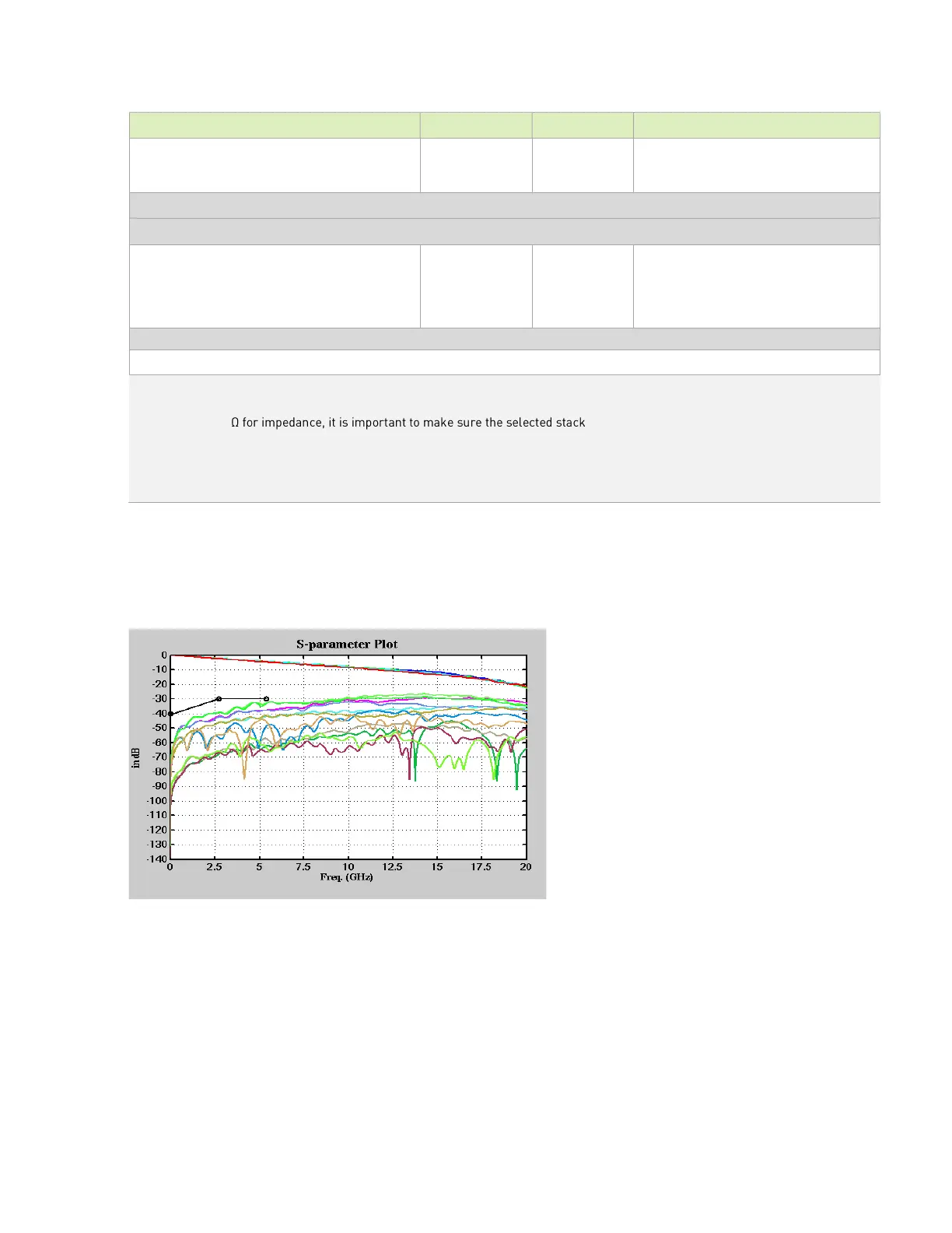
The following figures show the eDP and DP interface signal routing requirements.
Figure 9-4. S-Parameter Up to HBR2
 Loading...


