Display
PRELIMINARY INFORMATION
Jetson Orin NX Series and Jetson Orin Nano Series DG-10931-001_v1.1 | 48
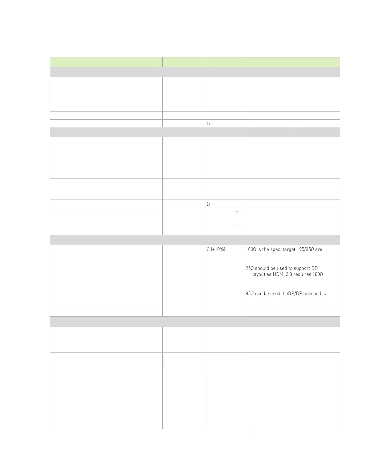
Table 9-3. eDP and DP Main Link Signal Requirements Including DP_AUX
Max Data Rate / Min UI
HBR3
HBR2
HBR
RBR
8.1 / 123
5.4 / 185
2.7 / 370
1.62 / 617
Number of Loads / Topology
Point-Point, Differential, Unidirectional
Insertion Loss
E-HBR @ 0.675GHz
PBR 0.68GHz
HBR 1.35GHz
HBR2 @ 2.7GHz
HBR3 @ 4.05GHz
<=0.7
<=0.7
<=1.2
<=4.5
<=5.5
Resonance dip frequency
HBR2
HBR3
FEXT
@ DC
@ 2.7GHz
@ 5.4GHz
<= -40dB
<= -30dB
<= -30dB
IL/FEXT plot up to HBR2. See Figure 9-4.
IL/FEXT plot HBR3. See Figure 9-5.
Trace Impedance (Diff pair)
implementation options (Zdiff does not
account for trace coupling)
-HDMI
co-
impedance (see HDMI section for addition of
series resistor RS).
preferable as it provides better trace loss
characteristic performance. See Note 1.
Trace Length (delay), Spacing and Skew
Trace loss characteristic
HBR2 or lower (@ 2.7GHz)
HBR3 (@4GHz)
The following max length (delay) is derived
based on this characteristic. The length
(delay) constraint must be re-defined if loss
characteristic is changed.
Max PCB Via dist. from module conn.
RBR/HBR
HBR2 and HBR3
Max trace length (delay) from module to connector
RBR/HBR
Stripline
Microstrip
HBR2
Stripline
Microstrip
HBR3
215 (1137.5)
215 (975)
184 (1260)
178 (1050)
6.9ps/mm assumption for Stripline,
5.9ps/mm for Microstrip.
 Loading...


