NVIDIA Jetson TX2/TX2i OEM Product Design Guide
JETSON TX2/TX2i OEM PRODUCT | DESIGN GUIDE | 20180618 40
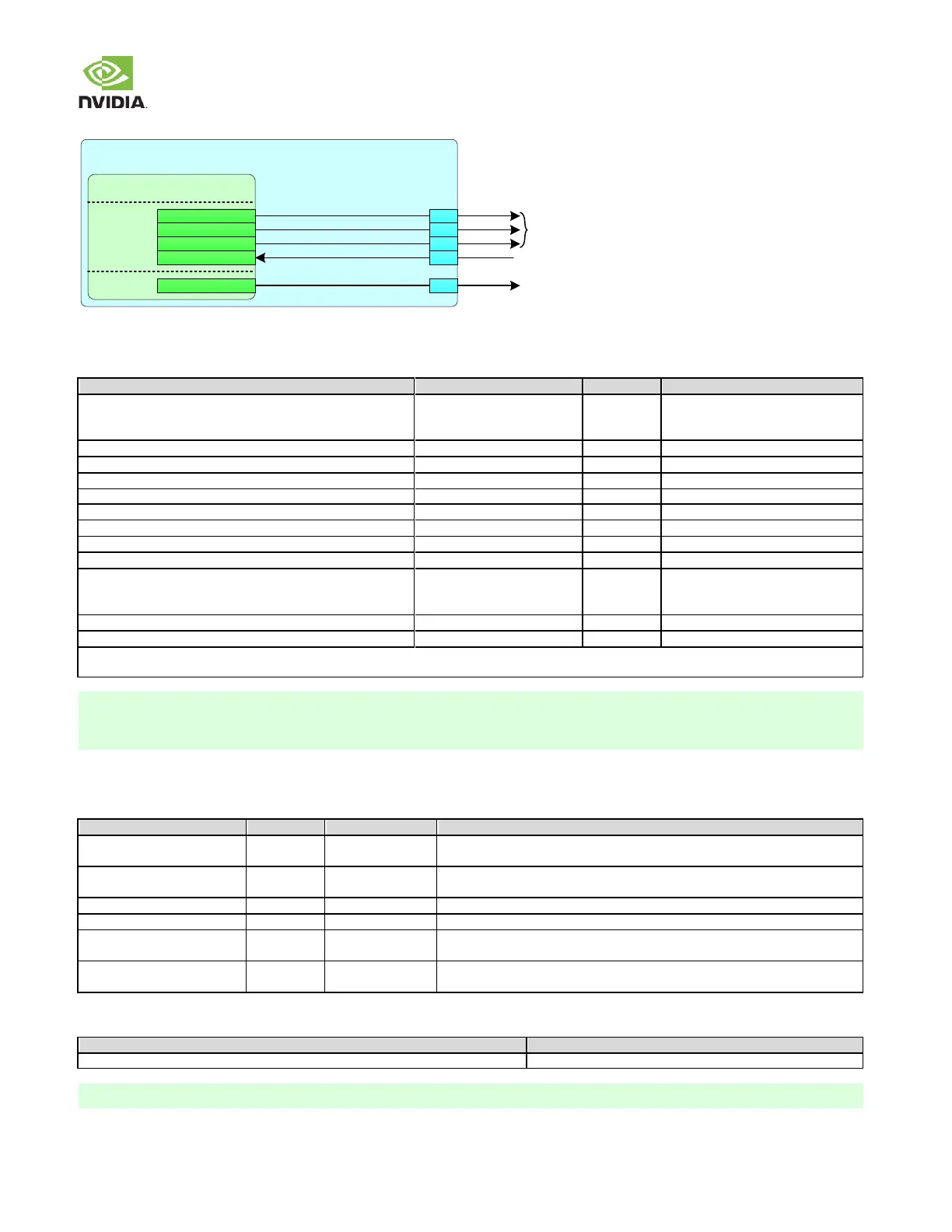
Figure 23: Display Backlight/Control Connections
Jetson TX2/TX2i
Tegra
LCD_BKLT_EN
LCD0_BKLT_PWM
LCD1_BKLT_PWM
LCD_TE
LCD_VDD_EN
eDP
GPIO_EDP0
SYS
GPIO_DIS3
GPIO_DIS0
GPIO_DIS5
GPIO_DIS1
Backlight
Control
B2 6
A25
B2 8
B2 7
A24
Tearing Effect
Display
Power Enable
MIPI DSI / CSI Design Guidelines
Table 35. MIPI DSI & CSI Interface Signal Routing Requirements
Max Frequency/Data Rate (per data lane) HS (DSI)
HS (CSI)
LP
Breakout Region Impedance (Single Ended)
Trace Impedance Diff pair / Single Ended
Via proximity (Signal to reference)
Trace spacing Microstrip / Stripline
Max Trace Delay 1 Gbps
1.5 Gbps
2.5 Gbps
Max Trace Delay Skew between DQ & CLK
Keep critical DSI/CSI related traces including DSI/CSI clock/data traces & RDN/RUP traces away from other signal traces or unrelated power
traces/areas or power supply components
1. If PWR, 0.01uF decoupling cap required for return current
2. Up to 4 signal Vias can share a single GND return Via
3. If routing to device includes a flex or 2nd PCB, the max trace & skew calculations must include all the PCBs/flex routing
MIPI DSI / CSI Connection Guidelines
Table 36. MIPI DSI Signal Connections
DSI Differential Clocks: Connect to CLKn & CLKp pins of receiver. See
connection diagrams for Dual & Split Link Mode configurations.
DSI Differential Data Lanes: Connect to Dn & Dp pins of DSI display. See
connection diagrams for Dual & Split Link Mode configurations.
LCD Tearing Effect: Connect to LCD Tearing Effect pin if supported
LCD Backlight Enable: Connect to LCD backlight solution enable if supported
LCD Backlight Pulse Width Modulation: Connect to LCD backlight solution PWM
input if supported
LCD Power Enable: Connect as necessary to enable appropriate Display power
supply(ies).
Table 37. Recommended DSI observation (test) points for initial boards
One for each signal line.
Near display. Panel connector pins can be used if accessible.
Test points must be done carefully to minimize signal integrity impact. Avoid stubs & keep pads small & near signal traces