NVIDIA Jetson TX2/TX2i OEM Product Design Guide
JETSON TX2/TX2i OEM PRODUCT | DESIGN GUIDE | 20180618 56
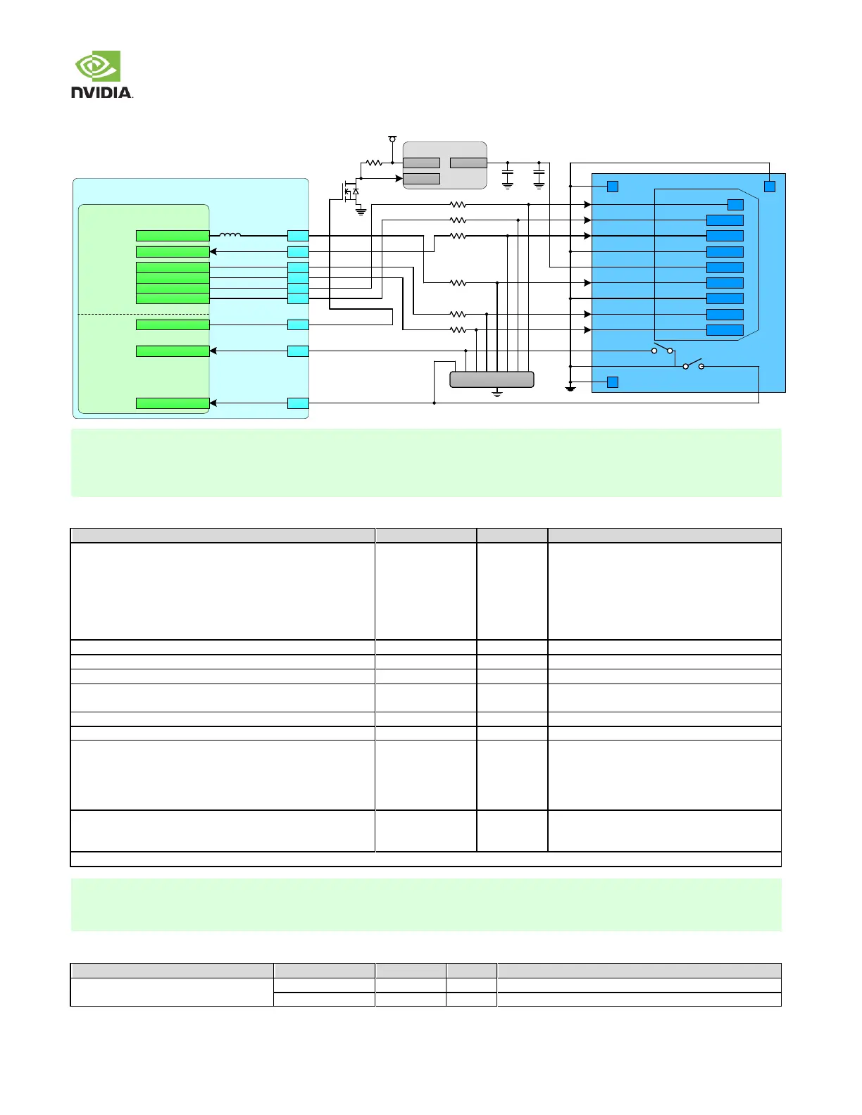
Figure 31. SD Card Socket Connection Example
Jetson TX2/TX2i
SDMMC1_ CD*
Tegra
SDMMC1
SDMMC1_CLK
SDMMC1_CMD
GPIO_EDP1
EDP
ESD
DATA2
DATA3
CMD
VDD
CLK
GND
DATA0
DATA1
C_DETECT
COMMON
VDD_3V3_SYS
SDMMC1_DAT3
Load Switch
VOUTVIN
ON
SDMMC_VDD_EN
GPIO_EDP2
GND
GPIO_EDP3
SDMMC1_ WP
C_WR_PROTECT
SDCARD_CLK
SDCARD_CMD
SDCARD_D0
SDCARD_D1
SDCARD_D2
SDCARD_D3
SDCARD_PWR_EN
SDCARD_CD#
SDCARD_WP
SDMMC1_DAT2
SDMMC1_DAT1
SDMMC1_DAT0
G19
G18
F17
H16
F20
H18
H17
F19
F18
10
10
10
0
10
10
MHz
4.7k
G
S
D
1. If EMI and/or ESD devices are necessary, they must be tuned to minimize the impact to signal quality, which must meet
the timing & Vil/Vih requirements at the receiver & maintain signal quality and meet requirements for the frequencies
supported by the design.
2. Supply (load switch, etc) used to provide power to the SD Card must be current limited if the supply is shorted to GND.
Table 54. SDCARD / SDIO Interface Signal Routing Requirements
Max Frequency 3.3V Signaling DS
HS
1.8V Signaling SDR12
SDR25
SDR50
SDR104
DDR50
25 (12.5)
50 (25)
25 (12.5)
50 (25)
100 (50)
208 (104)
50 (50)
-up
Independand of stackup layers
Depends on stackup layers
Via proximity (Signal to reference)
Up to 4 signal Vias can share 1 GND return Via
Trace spacing Microstrip / Stripline
Trace length
SDR50 / SDR25 / SDR12 / HS / DS Min
Max
SDR104 / DDR50 Min
Max
16 (100)
139 (876)
16 (100)
83 (521)
Max Trace Delay Skew in/between CLK & CMD/DAT
SDR50 / SDR25 / SDR12 / HS / DS
SDR104 / DDR50
Keep CLK, CMD & DATA traces away from other signal traces or unrelated power traces/areas or power supply components
1. Actual frequencies may be lower due to clock source/divider limitations.
2. If PWR, 0.01uF decoupling cap required for return current.
3. If routing to SD Card socket includes a flex or 2nd PCB, max trace & skew calculations must include PCB & flex routing.
Table 55. SD Card Loading vs Drive Type
General SD Card Compliance