NVIDIA Jetson TX2/TX2i OEM Product Design Guide
JETSON TX2/TX2i OEM PRODUCT | DESIGN GUIDE | 20180618 64
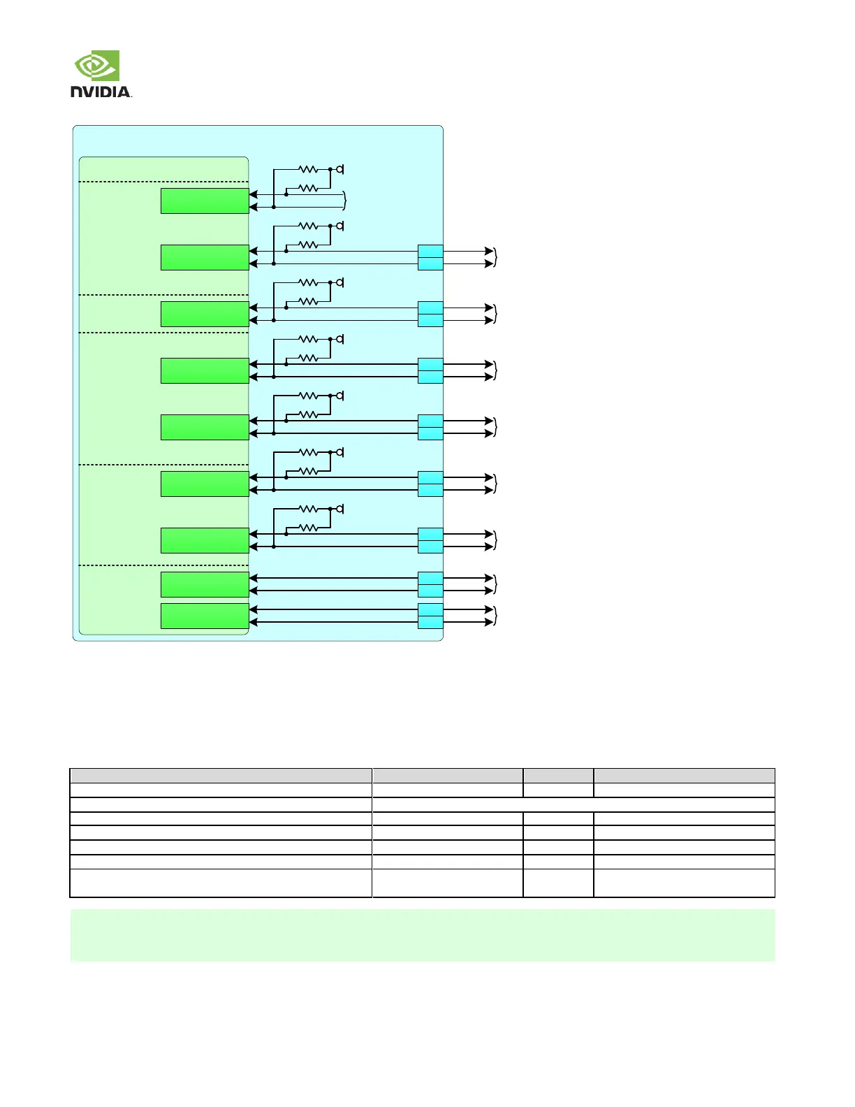
Figure 35. I2C Connections
Jetson TX2/TX2i
Tegra I2C
PWR_I2C_SCL
PWR_I2C_SDA
CAM_I2C_SCL
CAM_I2C_SDA
SYS
GEN9_I2C_SCL
GEN9_I2C_SDA
On-Module
Usage Only
VDD_1V8
CAM
UART
1k
GEN1_I2C_SCL
GEN1_I2C_SDA
AO
GPIO_SEN8
GPIO_SEN9
DP_AUX_CH0_P
DP_AUX_CH0_N
DP
DP_AUX_CH1_P
DP_AUX_CH1_N
1k
VDD_1V8
1k
1k
VDD_1V8
1k
1k
VDD_1V8
1k
1k
VDD_3V3_SYS
1k
1k
Used as camera module
control interface
I2C_GP1_CLK
I2C_GP1_DAT
I2C_CAM_CLK
I2C_CAM_DAT
I2C_GP2_CLK
I2C_GP2_DAT
I2C_GP3_CLK
I2C_GP3_DAT
I2C_GP0_CLK
I2C_GP0_DAT
I2C_PM_CLK
I2C_PM_DAT
DP0_AUX_CH+
DP0_AUX_CH
DP1_AUX_CH+
DP1_AUX_CH
Available for misc.
1.8V I2C devices
Used on-module for power monitors, & typically off-
module for GPIO expansion or other misc 3.3V I2C usage
Typically used for eDP. Otherwise
available for Misc 1.8V/3.3V I2C usage.
Typically used for HDMI or DP. Otherwise
available for Misc 1.8V/3.3V I2C usage.
D6
C6
A6
B6
E15
D15
B3 5
B3 4
A34
A35
A21
A20
C11
C10
C12
C13
GEN8_I2C_SCL
GEN8_I2C_SDA
VDD_1V8
1k
1k
I2C2
I2C6
I2C5
I2C1
I2C3
I2C4
I2C9
I2C8
GEN7_I2C_SCL
GEN7_I2C_SDA
VDD_1V8
1k
1k
Available for misc.
1.8V I2C devices
I2C7
Available for misc.
1.8V I2C devices
Available for misc.
1.8V I2C devices
I2C Design Guidelines
Care must be taken to ensure I2C peripherals on same I2C bus connected to the module do not have duplicate addresses.
Addresses can be in tw o forms: 7-bit, w ith the Read/Write bit removed or 8-bit including the Read/Write bit. Be sure to compare
I2C device addresses using the same form (all 7-bit or all 8-bit format).
Table 68. I2C Interface Signal Routing Requirements
Max Frequency Standard-mode / Fm / Fm+
Single ended, bi-directional, multiple masters/slaves
Max Loading Standard-mode / Fm / Fm+
Max Trace Delay Standard Mode
Fm & Fm+
1. Fm = Fast-mode, Fm+ = Fast-mode Plus
2. Avoid routing I2C signals near noisy traces, supplies or components such as a switching power regulator.
3. No requirement for decoupling caps for PWR reference