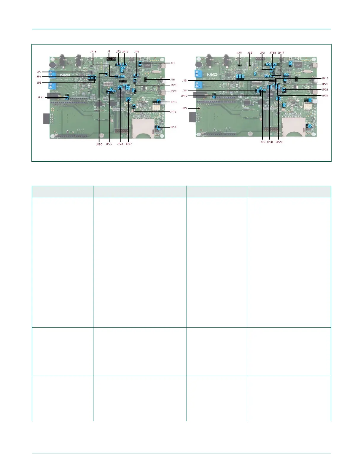
Figure 3. i.MX RT685 EVK jumpers and headers
Table 2 provides a description of jumpers and indicators.
Table 2. Indicators and jumpers
Circuit ref (Rev E) Description Default Reference
JP1
Link2 (LPC43xx) force DFU boot.
Leave this jumper open (default) for
Link2 to follow the normal boot
sequence. The Link2 will boot from
flash if image is found there. With the
flash erased the Link2 normal boot
sequence will fall through to DFU boot.
Install this jumper to force the Link2 to
DFU boot mode. Use this setting to
reprogram the Link2 internal flash with
a new image (using the LPCScrypt
utility) or to use the MCUXpresso IDE
with CMSIS-DAP protocol.
The Link2 flash is pre-programmed
with a version of CMSIS-DAP firmware
by default.
Open Schematic
JP2
Buffer Power Selection
For On-board Target place in position
1-2 (default)
For Off-board Target place in position
2-3
1-2 Schematic
JP3
Target processor selection for the on-
board Debug Probe.
Jumper open (default) the i.MX RT685
Target SWD interface enabled.
Normal operating mode where the
Open Schematic
Table continues on the next page...
NXP Semiconductors
Board layout and settings
i.MX RT685 Evaluation Board, Rev. 0, March 20 2020
User's Guide 8 / 31
 Loading...


