Home
NXP Semiconductors
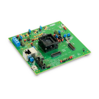
Motherboard
S32R274
Page 24 (Test Points - Daughter Card)
NXP Semiconductors S32R274 - Test Points - Daughter Card
40 pages
Manual
To Next Page
To Next Page
To Previous Page
To Previous Page
Loading...
Configuration
–
Daughter card
S32R274/
372 EV
B User G
uide
, Re
v. 0, 08/
2018
24
NXP Semiconductors
4.10.
Test points - daughter card
Daughter card test points are listed and detailed in the table below.
Table 11.
Test points
–
daugh
ter card
Signal
TP
name
Shape
Description
VREG_SWP
TP1
Test Loop
Driver signal for
external switching
transistor
3V3_HV_REG
TP2
Test Loop
3V3 Supply to external
transistor
VREG_I-SENSE
TP3
Test Loop
Current sense analog
input
3V3_PGOOD
TP4
Surface Pad
Power good signal from
3.3v linear regulator
4V2_PGOOD
TP5
Surface Pad
Power good signal from
4.2v switching regulator
4V2_SW_REG
TP6
Surface Pad
4.2V Switching regulator
output
1V2_LR_HV
TP7
Surface Pad
1.2V Ethernet phy
regulator output
1.25V_SR_LDO
TP8
Surface Pad
1.25V Core supply
VDD_LV_RADARDIG
TP9
Surface Pad
1.4V RADAR Reference
VDD_LV_RADARREF
TP10
Surface Pad
1.4V RADAR Reference
VDD_HV_RAW
TP11
Surface Pad
Analog supply for 1.4v
on chip regulators
VDD_HV_DAC
TP12
Surface Pad
3.3V Analog supply for
DAC
VDD_HV_DAC_2V5
TP13
Surface Pad
2.5V supply voltage for
DAC
AFE_FILTER
TP14
Surface Pad
AFE filter
GND
TP28,
TP29
Test Loop
Ground
ETIMER2_ETC0
TP30
Test Loop
Etimer 2 Channel 0
NPC_EVTO_B
TP31
Test Loop
PI9 (Pad G14)
VDD_LV_SDPLL
TP32
Surface Pad
1.4V Analog supply for
320Mhz PLL
VDD_LV_SDADC
TP33
Surface Pad
1.4V analog supply for
SD ADCs
VDD_LV_OSC
TP34
Surface Pad
1.4V analog supply for
crystal oscillator
ENET_REF_CLK
TP35
Test Loop
125MHz ENET
Reference clock
23
25
Table of Contents
Main Page
1 Introduction
1
Table of Contents
1
List of Acronyms
1
Modular Concept
2
Daughter Card Availability
3
2 EVB Features
3
3 Configuration
5
Power Supply Configuration
5
CAN Configuration
8
RS232 Configuration
9
LIN Configuration
10
Flexray Configuration
11
Ethernet Configuration
12
Motherboard
12
4 Configuration - Daughter Card
14
MCU Power
15
Reset Circuit
17
MCU External Clock Circuit
18
Jtag
19
Nexus Aurora
20
Serial Interprocessor Interface (SIPI)
20
Camera Serial Interface (MIPI-CSI2)
21
Gigabit Ethernet
21
Can Fd
23
Test Points - Daughter Card
24
Configuring the Daughter Card for Standalone Use25
25
Configuring External VREG Mode
25
Configuring Internal VREG Mode
26
5 Board Interface Connector
27
6 Default Jumper Summary Table
35
Default Jumper Table - Motherboard
35
User Area
38
Known Issues
38
Related product manuals
NXP Semiconductors S32K142
45 pages
NXP Semiconductors S32K148
24 pages
NXP Semiconductors S32K144 EVB
45 pages
NXP Semiconductors S32K116 EVB
45 pages
S32K312EVB-Q172
25 pages
S32K3X4EVB-Q172
31 pages
NXP Semiconductors MPC5777C
60 pages
NXP Semiconductors MIMXRT1060
19 pages
NXP Semiconductors QorIQ T1040
68 pages
NXP Semiconductors MPC57 Series
22 pages
NXP Semiconductors QorIQ LX2160A
137 pages
LPCXpresso55S69
25 pages
 Loading...