Do you have a question about the NXP Semiconductors QorIQ T1040 and is the answer not in the manual?
| Processor | QorIQ T1040 |
|---|---|
| Architecture | Power Architecture |
| Cores | 4 |
| Clock Speed | 1.4 GHz |
| Security Engine | Yes |
| Manufacturing Process | 28 nm |
| Memory Support | DDR3/DDR3L |
| Max Memory | 8 GB |
| PCI Express | 2.0 |
| USB Ports | 2 |
| SATA Ports | 2 |
| Operating Temperature | -40 to 105 °C |
Lists and describes related documents available under NDA, contact for access.
Defines technical terms and abbreviations used in the document for clarity.
Briefly describes the silicon features, referring to another manual for details.
Lists the main features of the T1040RDB board, including SerDes, DDR, Ethernet, CPLD, and clocks.
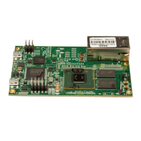
Provides a high-level overview of the T1040 SoC and T1040RDB board functional units.
Explains the processor support on the T1040RDB, focusing on signal isolation.
Describes the power supply system using an ATX PSU, outlining goals and architecture.
Details the clock circuitry providing clocks for the processor and other components.
Explains how the CPLD manages reset signals for the T1040 processor and other board devices.
Details the T1040RDB's support for high-speed DDR3L DRAM, including socket type and ranks.
Describes the eight high-speed serial communication lanes supporting various protocols like SGMII, PCIe, and SATA.
States the T1040RDB supports PCIe evaluation using standard Gen 1/Gen 2 cards.
Explains the T1040RDB supports SGMII protocol evaluation using the RTL8211DN PHY.
Details the T1040RDB's QSGMII protocol evaluation using an F104S8A four-port Ethernet PHY.
Mentions SATA evaluation is possible via an onboard SATA connector.
Discusses the T1040's two Ethernet controllers (EC1, EC2) operating in RGMII mode.
Explains the use of the Ethernet management interface (EMI1) with onboard RGMII, SGMII, and QSGMII PHYs.
Details the four I2C buses and their use for accessing onboard devices and slots.
Outlines the purposes of the T1040 serial peripheral interface (SPI) for memory and device access.
Describes the T1040 Integrated Flash Controller (IFC), also known as the local bus, for managing devices.
Explains the enhanced SD host controller (eSDHC) providing an interface for SD/MMC cards.
Details the board's two integrated USB 2.0 controllers, their features, and connectivity.
Describes the T1040's two UART controllers providing RS-232 serial interconnection.
Explains the T1040 TDM interface connection to dual SLIC/SLAC devices for voice applications.
Details the JTAG/COP port for system debugging, including probe and debugger options.
Introduces the section covering connectors, headers, jumpers, push buttons, and LEDs on the platform.
Lists various connectors on the T1040RDB platform and their uses.
Lists headers on the T1040RDB platform and their purpose.
Describes the usage of jumpers on the T1040RDB platform for configuration.
Details how push buttons are used on the T1040RDB platform.
Lists the LEDs on the T1040RDB board, their identifiers, colors, uses, and controllers.
Explains the thermal monitoring using ADT7461, its connection to CPLD for fan control.
Describes the user-selectable DIP switches for evaluating boot configurations and special settings.
Provides steps to program the CPLD using Altera USB-blaster and Quartus II software.
Presents the CPLD memory map, listing registers, addresses, access types, and reset values.
Details the Chip ID1 register, its address, bit fields, and description for CPLD image identification.
Details the Chip ID2 register, its address, bit fields, and description for CPLD image identification.
Describes the Hardware Version register, its address, and dependency on PLD image revision.
Details the Software Version register, its address, and dependency on PLD image version.
Explains the Reset Control Register 1 (RSTCON1), its bits, and their function in controlling resets.
Details the Reset Control Register 2 (RSTCON2), its bits, and their function in controlling various resets.
Describes the Interrupt Status Register (INTSR), its bits, and the interrupt sources.
Details the Flash Control and Status Register (FLHCSR) for boot selection and bank selection.
Explains the Fan Control and Status Register (FANCSR) for controlling fan PWM duty cycle.
Describes the Panel LED control register, indicating the status of various LEDs on the board.
Indicates that the SFP+ control and status register is reserved.
Details the Miscellaneous Control and Status Register for various settings like sleep mode, slot detection.
Explains the Boot Configuration Override register to enable/disable CPLD override of boot configuration.
Details the Boot Configuration Register 1 (BOOTCFG1) for RCW source selection.
Details the Boot Configuration Register 2 (BOOTCFG2) for RCW source bit and other configuration bits.
Guides on preparing the T1040RDB for use, including serial console setup and settings.
Shows the mapping of Ethernet ports to Linux, U-Boot, and front-panel labels.
Explains how NOR flash is divided into banks for storing main and backup images.
Defines default switch settings and other boot source settings for the board.
Specifies the default switch settings for NOR flash boot.
Defines switch settings for NAND boot, SPI boot SW, and SD boot.
Provides a detailed description of the switch settings for various boot configurations.
Directs users to SDK documentation for information on build details.
Explains how to flash and update images on the board for different boot sources.
Details the process of flashing images onto NOR flash and booting from it.
Provides steps for flashing and updating images for eSPI boot.
Outlines the steps for flashing and updating images for NAND boot.
Guides on flashing and updating images for SD card boot.
Explains how to boot Linux from U-Boot prompt with 32-bit and 64-bit configurations.


