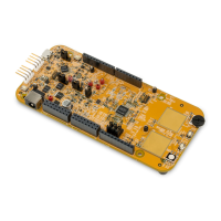
Default jumper summary table
S32R274/372 EVB User Guide, Rev. 0, 08/2018
38 NXP Semiconductors
6.2. User qrea
There is a rectangular prototype area on the motherboard top right corner, consisting of a 0.1 inch pitch
array of through-hole plated pads. Power from all the three switching regulators is readily accessible
along with GND through JP1 – JP16 next to the prototyping area. This area is ideal for the addition of
any custom circuitry.
There are four active low user LEDs D2, D3, D4 and D5, these are driven by connecting a logic 0 signal
to the corresponding pin on 0.1” header P7 (USER LEDS). The LED inputs are pulled to
VDD_HV_IO_MAIN through 10kOhm resistors.
There are f active high pushbutton switches SW1, SW2, SW3 and SW4 which will drive 5 V onto the
respective pins on 0.1” connector P6 when pressed. The switch outputs are pulled to GND via 10kOhm.
Potentiometer RV1 can be connected to port pin PB[0] and is adjustable between GND and 5V from the
linear regulator. Power from all regulators can be connected to port pins as through J54:
• 1-2: 1.25V_SR to PB[1]
• 3-4: 3.3V_SR to PB[2]
• 5-6: 5V_SR to PB[3]
• 7-8: 5V_LR to PB[4]
The P12V rail from the 12 V input is scaled to 4.3 V through the voltage divider of R81 and R82 and the
scaled voltage can be connected to PB[5] via J55.
6.3. Known issues
No known issues.
 Loading...