5G Module Series
RM500Q-AE&RM502Q-AE Hardware Design
RM500Q-AE&RM502Q-AE_Hardware_Design 41 / 83
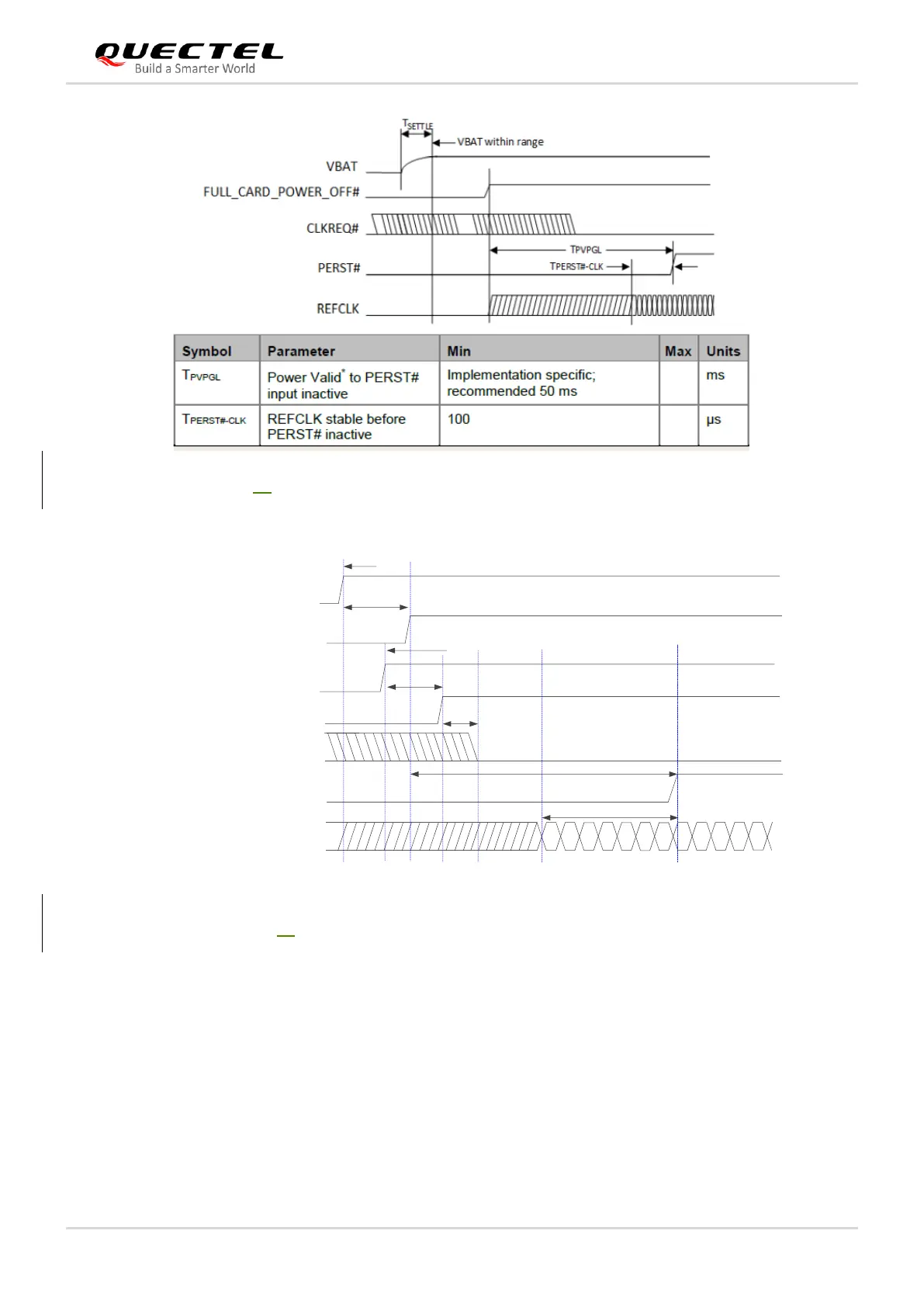
Figure 18: PCIe Power-on Timing Requirements of M.2 Specification
Figure 19: PCIe Power-on Timing Requirements of the Module
The following principles of PCIe interface design should be complied with, so as to meet PCIe
specification.
⚫ Keep the PCIe data and control signals away from sensitive circuits and signals, such as RF, audio,
crystal and oscillator signals.
⚫ Add a capacitor in series on Tx/Rx traces to prevent any DC bias.
⚫ Keep the maximum trace length less than 300 mm.
⚫ Keep the length matching of each differential data pair (Tx/Rx) less than 0.7 mm for PCIe routing
traces.