User’s Manual 71
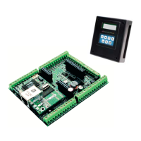
A.5 I/O Address Assignments
Table A-4 lists the external I/O addresses for the digital inputs and outputs.
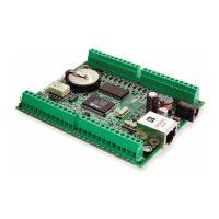
PE1 serves as a system-enable control. When PE1 is high or in a high-impedance status,
all BL2100 outputs are disabled (digital outputs and analog outputs are disabled, and
RS-485 is at listen status).
PE0 is configured as a strobe and is used for digital inputs, digital outputs, and the control
register. The control register is located at 0xx4–0xx7, write only. The function of each bit
is listed in Table A-5.
PA0–PA7 are used with IN16–IN23, which may be reconfigured as sinking digital outputs
OUT16–OUT23 by installing/removing components as reflected in the schematic.
All analog inputs and outputs are accessed by a series connection. PD3 is served as a clock
line while PB0 and PB7 are used for data in and data out, respectively.
PD4 and PD5 are used for RS-485 communication. The direction of the communication is
controlled by the control register. PC0, PC1, and PC2, PC3 are used for RS-232 communi-
cation. They can be used separately as two 3-wire RS-232, or they may be combined to
work as a 5-wire RS-232 port.
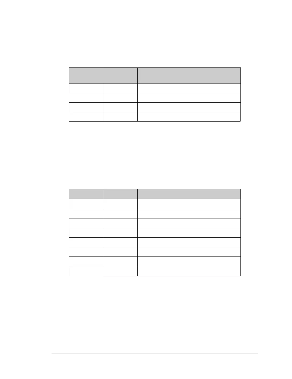
Table A-4. Digital I/O Addresses
External
Address
Name Function
0000 DIPA Digital inputs IN00–07, read only
0001 DOPA Digital outputs OUT00–OUT07, write only
0002 DIPB Digital inputs IN08–15, read only
0003 DOPB Digital outputs OUT08–OUT15, write only
Table A-5. Control Register Bit Map (External 0x0004–0x007)
Bit Name Function
0 485_SEND RS-485 send/receive
1 DO_CS0 Digital output 0–08, enable low active
2 DO_CS1 Digital output 09–16, enable low active
3 Not used Not used
4 AO_CS Analog output 00–04, enable low active
5 DAC_CS0 Chip select for analog ch 00 and 01
6 DAC_CS1 Chip select for analog ch 02 and 03
7 ADC_CS Chip select for A/D converter