TPS-1 User’s Manual: Hardware 2. Pin function
R19UH0081ED0107 Rev. 1.07 page 15 of 86
Jul 30, 2018
2.3. Supply Voltage Circuitry
The TPS-1 works with three operating voltages: VDD15 (1.5 V), VDD33 (3.3 V, IO) and VDD10 (1.0 V, core). Additionally, the on-chip PLL for the
device clock generation requires a supply called PLL_AVDD (1.0 V), which is typically a filtered version of VDD10. The integrated PHYs of the
TPS-1 require additional filtered operating voltages.
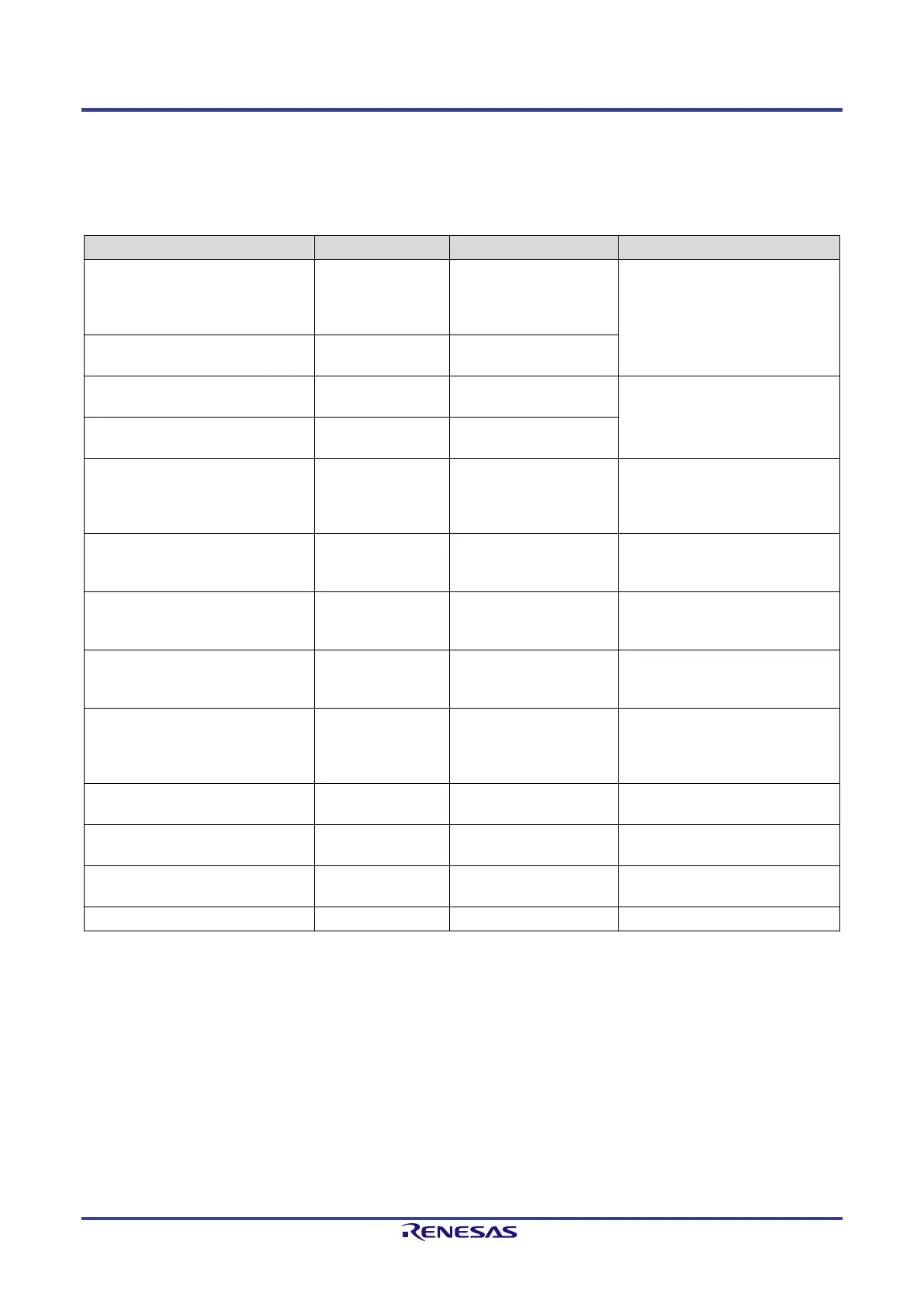
Table 2-3: Supply Voltage Circuitry
Supply Voltage Generation
D14,
L14
P1VDDARXTX
P2VDDARXTX
Analog port RX/TX
power supply, 1.5 V
(PHY port 1 and port
2)
Must be generated from
VDD15 via a filter.
supply, 1.5 V (PHY)
H14 VDDACB Analog central power
supply, 3.3 V (PHY)
Must be generated from
VDD33 via a filter.
supply, 3.3 V (PHY)
G13 VSSAPLLCB Analog central GND
(PHY)
Must be generated from GND
Core/IO via a filter or
connected to GND Core/IO at
the far end from TPS-1.
M8
VDDQ_PECL_B2
supply 3.3 V (port 1
and port 2)
L9 PLL_AGND Analog Ground for the
internal CPU clock
generation
internal CPU clock
generation (1.0V)
A1, A14, B7, F7, F8, F9, G6, G7,
G8, G9, G10, G12, H6, H7, H8,
H9, H10, J2, J6, J7, J8, J9, J12,
M10, N7, N10, P1, P14
GND Digital GND
PHYs
B1, B14, C7, F6, F10, H2, N1,
N14, P7, P10
VDD33 Voltage Supply 3.3 V External
A2, A7, A13, F12, K1, K12, M9,
P2, P13
form Switching Regulator or
external
E6, E7, E8, E9, K6, K7, K8, K9 VDD10 Voltage Supply 1.0 V External
 Loading...