EasyManuals Logo
Home>Renesas>Controller>TPS-1

Renesas TPS-1 User Manual

Renesas TPS-1
91 pages
To Next Page IconTo Next Page
To Previous Page IconTo Previous Page
Page #14 background imageLoading...
Page #14 background image
TPS-1 Users Manual: Hardware 2. Pin function
R19UH0081ED0107 Rev. 1.07 page 14 of 86
Jul 30, 2018
2.2. GPIO multiplexing
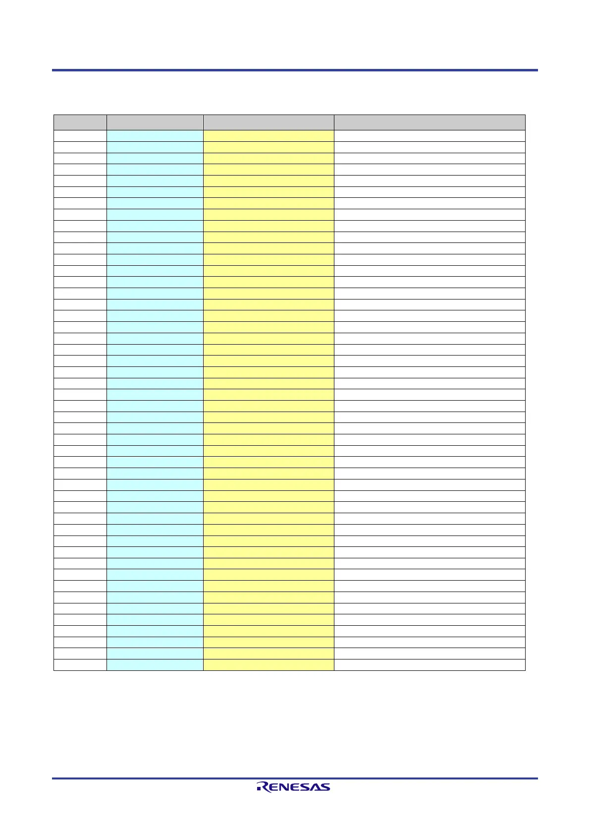
Table 2-2: Alternate use of the GPIOs
Pin
Designation
Alternate Use
Description
D5
GPIO 0
LBU WR EN IN
Write Enable
B5
GPIO 1
LBU READ EN IN
Read Enable
C5
GPIO 2
LBU CS IN
Chip Select
C4
GPIO 3
LBU BE 1 IN
Byte Selection (low)
A4
GPIO 4
LBU BE 2 IN
Byte Selection (high)
B4
GPIO 5
LBU READY OUT
Ready Signal TPS-1 (Note 1), (Note 2)
C3
GPIO 6
LBU DATA0
Data Bit
A3
GPIO 7
LBU DATA1
Data Bit
B3
GPIO 8
LBU DATA2
Data Bit
B2
GPIO 9
LBU DATA3
Data Bit
D3
GPIO 10
LBU DATA4
Data Bit
D4
GPIO 11
LBU DATA5
Data Bit
C1
GPIO 12
LBU DATA6
Data Bit
C2
GPIO 13
LBU DATA7
Data Bit
D2
GPIO 14
LBU DATA8
Data Bit
D1
GPIO 15
LBU DATA9
Data Bit
E2
GPIO 16
LBU DATA10
Data Bit
E3
GPIO 17
LBU DATA11
Data Bit
E4
GPIO 18
LBU DATA12
Data Bit
E5
GPIO 19
LBU DATA13
Data Bit
F5
GPIO 20
LBU DATA14
Data Bit
F4
GPIO 21
LBU DATA15
Data Bit
F3
GPIO 22
LBU A0 IN
Address Bit
G5
GPIO 23
LBU A1 IN
Address Bit
G4
GPIO 24
LBU A2 IN
Address Bit
H5
GPIO 25
LBU A3 IN
Address Bit
H4
GPIO 26
LBU A4 IN
Address Bit
J4
GPIO 27
LBU A5 IN
Address Bit
J3
GPIO 28
LBU A6 IN
Address Bit
K3
GPIO 29
LBU A7 IN
Address Bit
K4
GPIO 30
LBU A8 IN
Address Bit
K2
GPIO 31
LBU A9 IN
Address Bit
L2
GPIO 32
LBU A10 IN
Address Bit
L3
GPIO 33
LBU A11 IN
Address Bit
L1
GPIO 34
LBU A12 IN
Address Bit
M2
GPIO 35
LBU A13 IN
Address Bit
M1
GPIO 36
LBU SEG0 IN
Segment choice 1
M3
GPIO 37
LBU SEG1 IN
Segment choice 2
P3
GPIO 38
HOST RESET IN
Reset Host SPI Interface
N3
GPIO 39
HOST SFRN IN
Start new SPI Transfer (Note 3)
N2
GPIO 40
HOST SRXD IN
SPI receive data
N4
GPIO 41
HOST SCLK IN
SPI Clock
M4
GPIO 42
HOST STXD OUT
SPI transmit data
P4
GPIO 43
HOST SHDR OUT
Header recognized
N5
GPIO 44
LOCAL SCLK OUT
SPI Clock (SPI master IO interface)
M5
GPIO 45
LOCAL SFRN OUT
SPI Chip Select (SPI master IO interface)
M6
GPIO 46
LOCAL SRXD IN
SPI receive date (SPI master IO interface)
M7
GPIO 47
LOCAL STXD OUT
SPI transmit data (SPI master IO interface)
Note: You can only use one interface exclusively. It is not allowed to use e.g. the parallel and serial host interface at the same time.
Note 1): The “LBU_READY_OUT” is designed to connect only to one microcontroller. If you want to connect additional devices you must
add circuitry to realize the high-impedance state.
Note 2): If your processor does not have a READY Input, you can choose a wait time of 260 ns during each transfer cycle.
Note 3): As soon as the signal HOST_SFRN_IN is set to “1”, no more data is received on the RxD interface. Setting the signal is not allowed
during an ongoing transfer.

Table of Contents

Questions and Answers:

Question and Answer IconNeed help?

Do you have a question about the Renesas TPS-1 and is the answer not in the manual?

Renesas TPS-1 Specifications

General IconGeneral
BrandRenesas
ModelTPS-1
CategoryController
LanguageEnglish