TPS-1 User’s Manual: Hardware Appendix. B Board Design Information
R19UH0081ED0107 Rev. 1.07 page 77 of 86
Jul 30, 2018
Figure B-2: Change Tantalum to Ceramic Capacitor
Layout Example for Switching Regulator
This chapter shows an example for the connection between the external output and regulator. The real design of the layout must be done on the PCB
board.
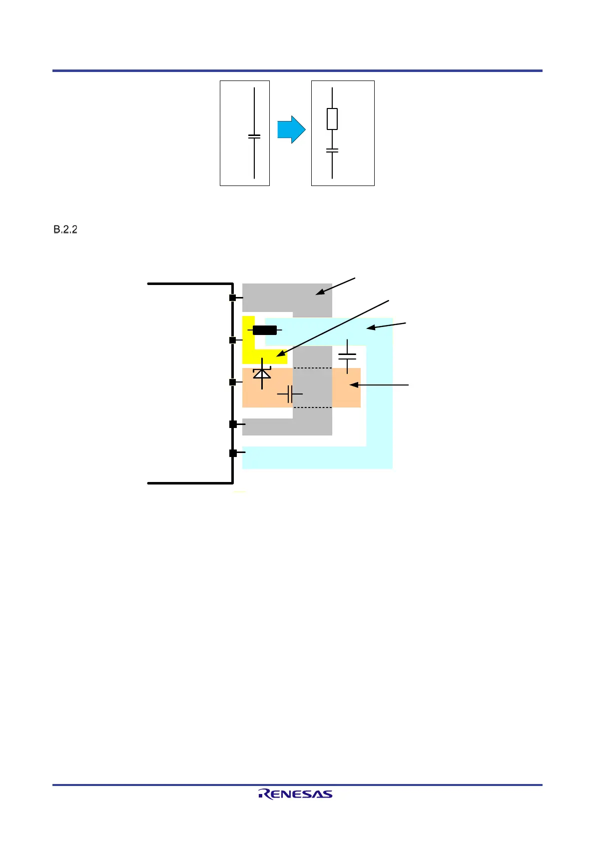
TPS-1
BVDD
Switching Regulator Input
(Pin J1, 3.3V)
LX
BGND (G1) /
AGND_REG (G2)
Regulator Ouput 1.5V
(Pin H1)
D1
GND for Switching
Regulator
Feedback Regulator
(Pin F1)
FB
AVDD_REG (F2)
L1: 10 uH
+
+
C1: 22 uF (Tantal)
LX Pattern
VOUT Pattern
(Connection to VDD15
Powerplane)
GND Pattern
AVDD, BVDD
Pattern
C2: 22 uF (Tantal)
Figure B-3: Switching Regulator layout example
Instead of the tantalum capacitors you can also use ceramic capacitors. Please refer to chapter B.2.1 .
 Loading...