TPS-1 User’s Manual: Hardware Appendix. B Board Design Information
R19UH0081ED0107 Rev. 1.07 page 83 of 86
Jul 30, 2018
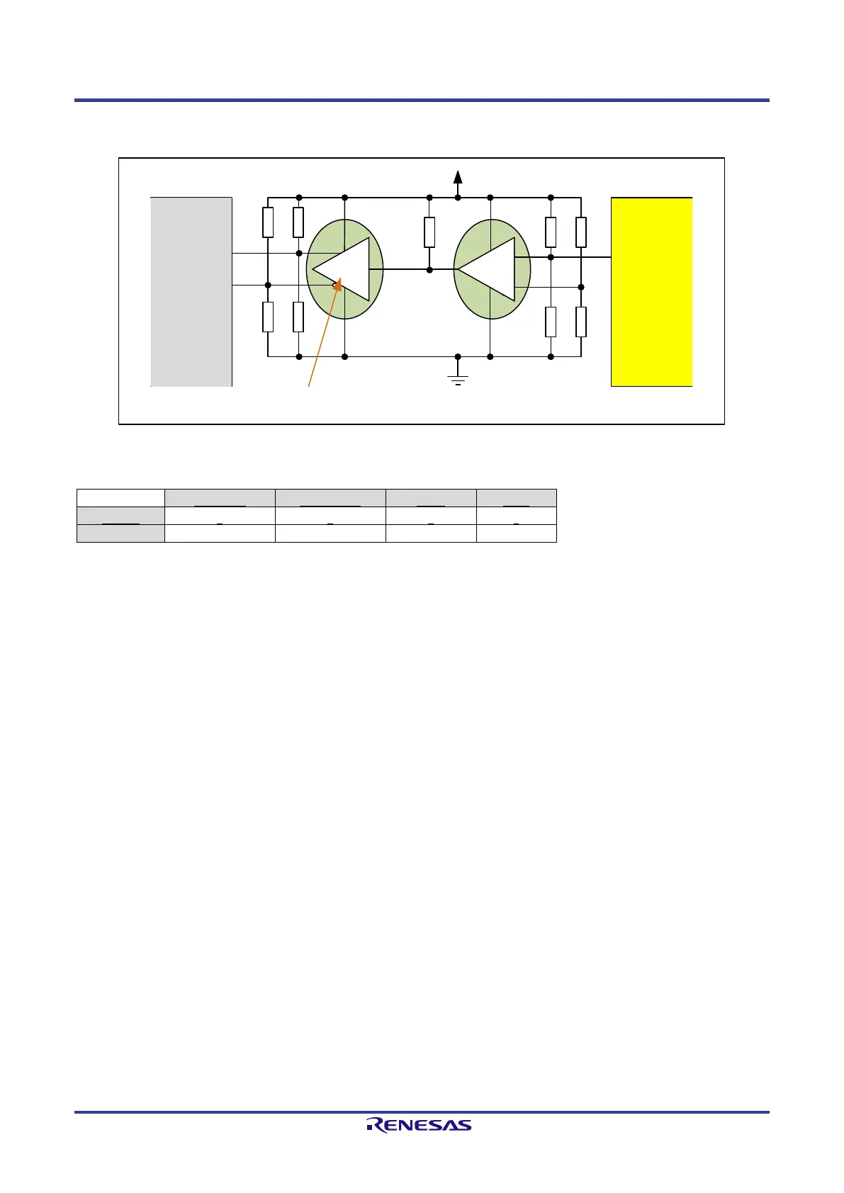
The circuitry for the connection of the SD-Pin of the transceiver to the SD_P/SD_N Pin of the TPS-1 is shown in Figure B-9. The active circuitry is
necessary because the QFBR/AFBR transceiver provides no differential signal.
SD-active circuitry
Transceiver
QFBR
SD
6
3
2
7
-
+
4
4K7
130R
130R
(1%)
191R
(1%)
82R
Vcc (3.3V,
tolerance +- 5%)
GND
6
1
2
7
5
130R 130R
82R 82R
TPS-1
Px_SD_P
Px_SD_N
LM293/TI
SN65LVELT22/TI
COMP_OUT
SD_N
SD_P
SD_Output
Figure B-9: Circuitry for the SD Signal
Table B-3: SD Signal for Transceiver
Using the AVAGO QFBR-5978Z or AFBR-5978Z Transceiver you must ensure the tolerance of the Supply Voltage (3.3V) between +- 5%.
Note: All resistors in this example should have a tolerance of 5% (see the exceptions).
If you want to use the FO diagnostic features, you can implement the AVAGO QFBR-5978AZ transceiver. For using the special features of this
transceiver you must connect the TPS-1 to the transceiver by an I2C-bus.
Receive and transmit lines are compliant to the LVPECL technology. These lines must be routed carefully to avoid influence from e.g. the I
2
C buses.
The power supply for the AVAGO transceiver is divided into the transmitter and receiver part. You need additional electronic components to reduce
noise. It is important to take care in the layout of the device board to achieve optimum performance from the transceiver. It is recommended to add a
filter to the power supply for the transmitter and receiver part.
 Loading...