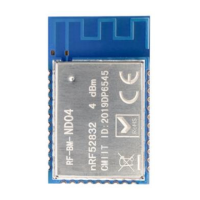
nRF52832
www.szrfstar.com V1.3 - Sep., 2020
Shenzhen RF-star Technology Co., Ltd. Page 5 of 58
Table of Figures
Figure 1. Multi-Connection Diagram ................................................................................................................ 10
Figure 2. PCB Footprint of RF-BM-ND04 ...................................................................................................... 11
Figure 3. PCB Footprint of RF-BM-ND04I ..................................................................................................... 11
Figure 4. Pin Assignment of RF-BM-ND04(I) ............................................................................................... 12
Figure 5. PCB Footprint of RF-BM-ND08 ...................................................................................................... 14
Figure 6. PCB Footprint of RF-BM-ND08I ..................................................................................................... 14
Figure 7. Pin Assignment of RF-BM-ND08(I) ............................................................................................... 15
Figure 8. Specification of Antenna Seat ......................................................................................................... 51
Figure 9. Specification of IPEX Wire ................................................................................................................ 51
Figure 10. Antenna Output Mode Change ..................................................................................................... 52
Figure 11. Reference Design of RF-BM-ND04 ............................................................................................ 52
Figure 12. Recommendation of Antenna Layout ......................................................................................... 54
Figure 13. Recommended Reflow for Lead Free Solder ......................................................................... 56
Figure 14. Optional Packaging Mode .............................................................................................................. 56