EasyManua.ls Logo

Samsung CT566BVX/STR User Manual

Samsung CT566BVX/STR
66 pages
To Next Page IconTo Next Page
Page #1 background imageLoading...
Page #1 background image
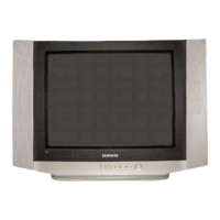
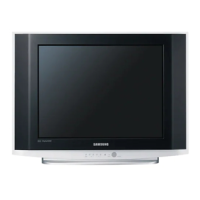
COLOR TELEVISION RECEIVER
Chassis : KCT57A
Model: CT566BVX/STR
CT566BVX/XAP
CT566BWX/STR
CT567BWX/STR
CT567BWX/XAP
CT766DWX/STR
CT766DWX/XAP
COLOR TELEVISION RECEIVER CONTENTS
Precautions
Specifications and IC Data
Alignment and Adjustment
Troubleshooting
Exploded View and Parts List
Electric Parts List
Block Diagram
PCB Layout Diagram
Wiring Diagram
Schematic Diagrams
1.
2.
3.
4.
5.
6.
7.
8.
9.
10.

Questions and Answers:

Samsung CT566BVX/STR Specifications

General IconGeneral
BrandSamsung
ModelCT566BVX/STR
CategoryTV Receiver
LanguageEnglish

Summary

Precautions

1-1 Safety Precautions

Safety precautions to prevent hazards like electrical shock and X-rays.

1-2 Servicing Precautions

Guidelines for safe and correct servicing procedures.

1-3 Precautions for Electrostatically Sensitive Devices (ESDs)

Techniques to reduce component damage caused by static electricity.

Specifications and IC Data

2-1 Specifications

Technical specifications for various TV models, including system, channels, and power.

2-2 IC Line Up

List of integrated circuits used, their location numbers, specifications, and descriptions.

2-3 Semiconductor Base Diagrams

Illustrations showing the pin configurations and base diagrams of various semiconductor components.

2-4 One Chip TV-processor

Pin diagram and function description for the SDIL56 one-chip TV processor.

Alignment and Adjustments

3-1 Preadjustment

Initial adjustments required before proceeding to service mode adjustments.

3-2 Factory ("SERVICE") Mode

Procedure to enter and navigate the factory service mode for adjustments.

3-2-1 Adjustment

Details on accessing and performing various adjustments within the factory mode.

3-2-2 Test Pattern (Aging Mode)

Using test patterns to confirm convergence and purity adjustments.

3-2-3 V2 Tri-Norma Option Table

Option byte settings for V2 Tri-Norma models, detailing data and functions.

3-2-4 Factory Reset

Procedure to reset user controls to initial values via factory mode.

3-3-1 General

General guidelines for TV installation and adjustment, including picture and color settings.

3-3-2 Automatic Degaussing

Explanation of the automatic degaussing function and manual degaussing procedure.

3-3-3 High Voltage Check

Procedure for checking high voltage levels and associated size specifications.

3-3-4 FOCUS Adjustment

Steps to adjust the focus control for a clear picture.

3-3-5 B+ Line Check

Checking the B+ voltage in different power modes.

3-3-6 F/S (Fail Safe) Circuit Check

Procedure to verify the operation of the failsafe circuit.

3-3-7 Color Purity Adjustment

Step-by-step guide for adjusting color purity using magnets and yoke.

3-3-8 Center Convergence Adjustment

Procedure for adjusting the center convergence of the picture using magnets.

3-3-9 AGC Adjustment

Adjusting the Automatic Gain Control (AGC) for optimal signal reception.

3-3-10 AFT (VCO Adjustment)

Adjusting the Automatic Fine Tuning (AFT) or Voltage Controlled Oscillator (VCO).

3-3-11 White Balance Adjustment

Detailed steps for screen, brightness, contrast, and color adjustments.

Troubleshooting

4-1 No Raster and No Sound

Troubleshooting flowchart for cases with no picture and no sound.

4-2 No Raster (Sound OK)

Troubleshooting flowchart for no raster when sound is present.

4-3 No Vert Scan (Horizontal Line)

Troubleshooting flowchart for vertical scan issues, resulting in a horizontal line.

4-4 No Sound

Troubleshooting flowchart for issues where there is no audio output.

4-3 No Color

Troubleshooting flowchart for cases where the TV displays no color.

Exploded View and Parts List

5-1 CT566BVX/STR, CT566BVX/XAP, CT566BWX/STR

Exploded view and parts list for specific CT566 and CT567 models.

5-2 CT567BWX/STR, CT567BWX/XAP

Exploded view and parts list for specific CT567 models.

5-3 CT766DWX/STR, CT766DWX/XAP

Exploded view and parts list for specific CT766DW models.

Electric Parts List

6-1 Dissimilar Power Parts List

List of power supply components that differ across various TV models and screen sizes.

6-2 Part Description (P/D) According to Screen Size

Detailed part descriptions categorized by screen size and model.

6-3 CRT PCB PART (TDA6101Q IC)

List of parts for the CRT PCB, specifically referencing the TDA6101Q IC.

6-4 COMB FILTER OPTION

List of components related to the comb filter option.

6-5 AUDIO OUT OPTION

List of components related to the audio output options.

6-6 VIDEO OUT OPTION

List of components related to the video output options.

6-7 MONO STEREO OPTION

List of components for mono and stereo sound options.

6-8 SOUND OUTPUT OPTION

List of components related to sound output options for different models.

6-9 JACK

List of jacks used in the TV, including their specifications.

6-10 CT566BVX/STR (CT566BWX/STR AND CT566BVX/STR Dissimilar Parts)

Parts list highlighting differences for CT566BVX/STR compared to other models.

6-11 CT566BVX/XAP (CT566BWX/STR AND CT566BVX/XAP Dissimilar Parts)

Parts list highlighting differences for CT566BVX/XAP compared to other models.

6-12 CT567BWX/STR (CT566BWX/STR AND CT567BWX/STR Dissimilar Parts)

Parts list highlighting differences for CT567BWX/STR compared to other models.

6-13 CT567BWX/XAP (CT566BWX/STR AND CT567BWX/XAP Dissimilar Parts)

Parts list highlighting differences for CT567BWX/XAP compared to other models.

6-14 CT766DWX/STR (CT566BWX/STR AND CT766DWX/STR Dissimilar Parts)

Parts list highlighting differences for CT766DWX/STR compared to other models.

6-15 CT566BWX/STR Parts List

Complete parts list for the CT566BWX/STR model.

Block Diagram

7-1 KCT57A Block Diagram

Overall block diagram illustrating the interconnection of major components in the KCT57A chassis.

PCB Layout

8-1 PWB-MAIN

Printed circuit board layout for the main board, showing component locations.

8-2 PWB-CRT V/M

Printed circuit board layout for the CRT V/M board.

8-3 ASSY-PCB-F/AV

Printed circuit board layout for the AV interface board.

8-4 ASSY-PCB, A/V SIDE

Printed circuit board layout for the AV side of the chassis.

Wiring Diagram

9-1 KCT57A Wiring Diagram

Wiring diagram showing the connections between different assemblies for the KCT57A chassis.

Schematic Diagrams

10-1 MAIN 1/4

Schematic diagram part 1 of 4 for the main board, showing power and some signal paths.

10-2 MAIN 2/4

Schematic diagram part 2 of 4 for the main board, detailing IF and Chroma sections.

10-3 MAIN 3/4

Schematic diagram part 3 of 4 for the main board, covering deflection and control circuits.

10-4 MAIN 4/4

Schematic diagram part 4 of 4 for the main board, showing CRT drive and power output.

10-5 CT766DW (MAIN 1/4)

Schematic diagram part 1 of 4 for the CT766DW model.

10-6 CT766DW (MAIN 2/4)

Schematic diagram part 2 of 4 for the CT766DW model, detailing IF and Chroma.

10-7 CT766DW (MAIN 3/4)

Schematic diagram part 3 of 4 for the CT766DW model, covering deflection and control.

10-8 CT766DW (MAIN 4/4)

Schematic diagram part 4 of 4 for the CT766DW model, showing CRT drive and power.

Related product manuals