8
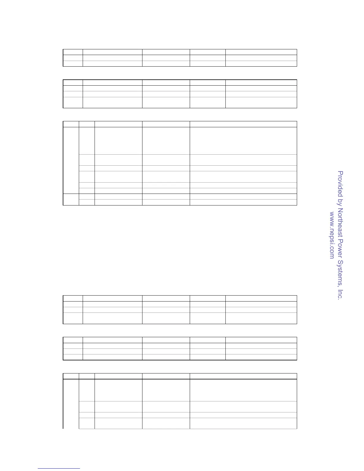
Table 2-1 Read Request Block
Bytes Description Range Type Notes
0,1 Command control See Table 2-3 UINT16
2,3 Start point ID 0x0000-0xFFFF UINT16
Table 2-2 Write Request Block
Bytes Description Range Type Notes
0,1 Command control See Table 2-3 UINT16
2,3 Start point ID 0x0000-0xFFFF UINT16
4-31 Data block INT16/INT32 32-bit integers occupy two 16-
bit words – most significant first
Table 2-3 Request Control
Byte Bits Description Range Notes
0-1 Operation 00=No operation
01=Read
10=Write
11=Clear
“Clear” and “No operation” remove the last master
command sent and clear the PROFIBUS input
buffer. After the device restarts, “Write” commands
are ignored until “Clear” or “Read” is sent first for
device synchronization.
2 Data type 0=32-bit integer
1=16-bit integer
32-bit integers occupy two 16-bit words – most
significant first
3 Unused
4 16-bit linear scaling 0=disabled
1=enabled
Only applied to 16-bit analog registers. Will not
affect binary registers and counters.
5-6 Unused
0
7 Synchronization bit 0-1 Toggle the bit to synchronize a response
0-3 Word count 1-14 Defines the number of words in the data block 1
4-7 Unused
Note: Bit 0 is a least significant bit (LSB).
Device Response Block
The device response block size can vary from 6 to 32 bytes. The actual block size is defined
when configuring the PROFIBUS master for this device by selecting the INTPUT module from
the device GSD file. The device response block formats are shown in Tables 2-4 and 2-5.
Successful read and write is acknowledged by the retransmission of bytes 0-3 of the master
request. Negative response is acknowledged by the retransmission of bytes 0-3 of the
master request with a non-zero exception code in byte 1. Note that the scaling bit in byte 0
may be dropped if there is actually no scaled data in the response message.
Table 2-4 Read Response Block
Bytes Description Range Type Notes
0,1 Response control See Table 2-6 UINT16
2,3 Start point ID 0x0000-0Xffff UINT16
4-31 Data block INT16/INT32 32-bit integers occupy two 16-
bit words – most significant first
Table 2-5 Write Response Block
Bytes Description Range Type Notes
0,1 Response control See Table 2-6 UINT16
2,3 Start point ID 0x0000-0xFFFF UINT16
4-31 Unused 0
Table 2-6 Response Control
Byte Bits Description Range Notes
0-1 Operation 00=data is not valid
01=read
10=write
11=data is not valid
“Data is not valid“ indicates that the data in the
device response block is not reliable and should not
be concerned
2 Data type 0=32-bit integer
1=16-bit integer
32-bit integers occupy two 16-bit words – most
significant first
3 Unused 0
0
4 16-bit linear scaling 0=no scaling
1=scaled data
Only 16-bit analog registers are affected. Binary
registers and counters are not scaled.
 Loading...