AL-1551CS ELECTRICAL SECTION 12 - 4
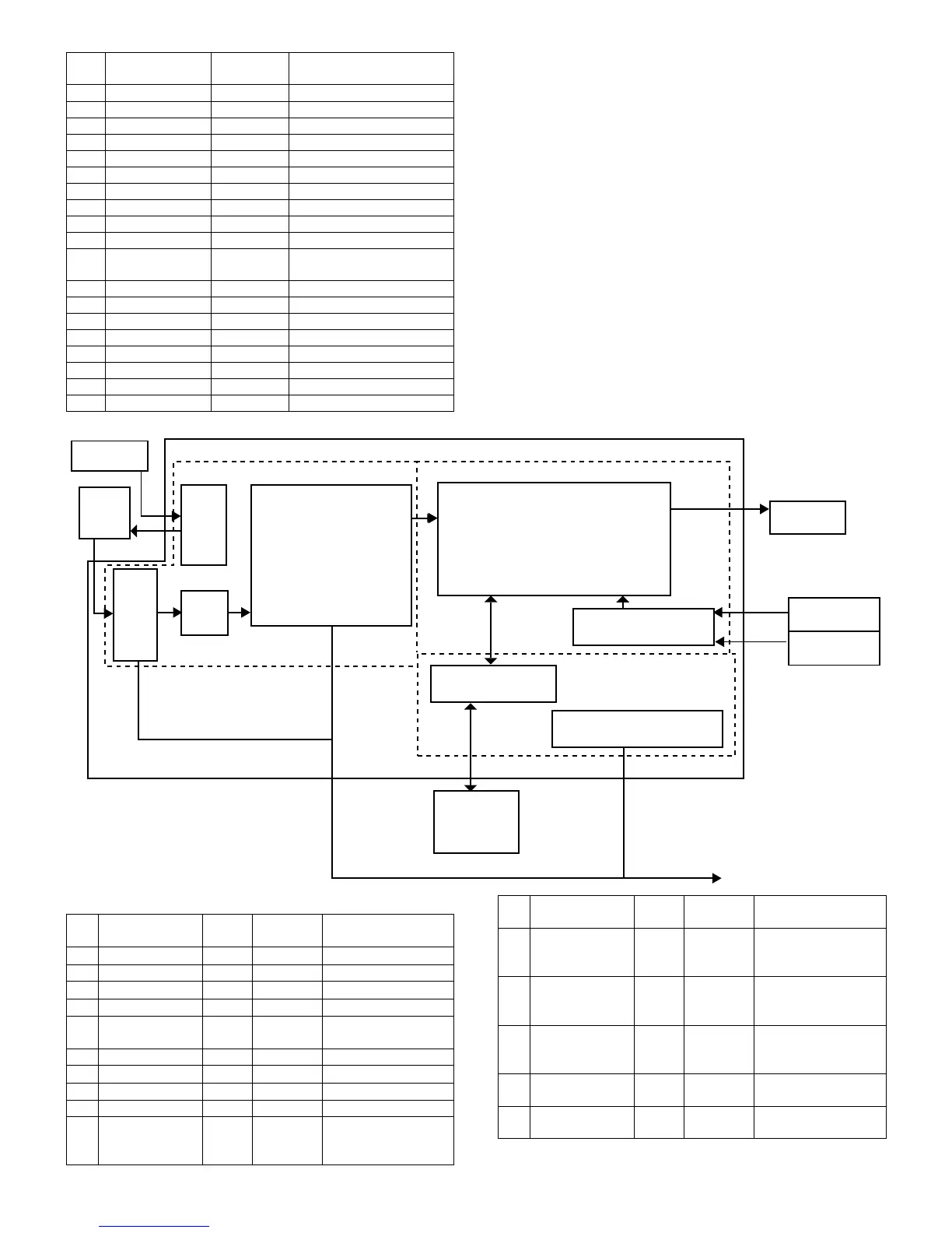
(3) Image process ASIC (HG73C119HF)
a. General
The ASIC is composed of the three major blocks: the image process
section, the print control section, and the I/F section.
Image process section:
With image data from the CCD PWB in the operation mode deter-
mined by the register setup, shading, AE process, input γ correc-
tion, area separation, filter process, resolution conversion, zoom
process, output γ correction, binary conversion (error diffusion,
dither method, simple binary conversion) are performed.
Print control section:
When copying, the image-processed data are outputted to the LSU
according to the LSU writing timing. When scanning, the image
data are made into 8bit width and outputted to the I/F section
(USB).
I/F section:
Controls the DRAM which is the image data buffer, and processes
data send/receive between the USB I/F and the IEEE1284 I/F.
The ASIC is controlled by writing the operation mode and the neces-
sary setup values of the operation mode into the ASIC control register
before starting each operation. (For ASIC Pin configuration, refer to the
table at the end of this document.)
b. ASIC (Signal table)
110 USBIN Input IF PWB detection signal
111 Input NC
112 Input NC
113 Avss DGND
114 GND DGND
115 /SCANSP Output Scan STOP signal
116 /SCANST Output Scan START signal
117 /TRANSST Output ASIC transfer signal
118 /PRINTST Output Print Start signal
119 SPMT3 Output SPF motor signal
120 SPMT2/MIRCNT Output/
Input
SPF motor signal/mirror
counter
121 SPMT1 Output SPF motor signal
122 SPMT0 Output SPF motor signal
123 GND DGND
124 GND DGND
125 Vcc CPU3.3V
126 PSL Output Power save LED control
127 NC
128 /CS2 Output ASIC chip select
PIN
No.
Signal code
Input/
Output
Operating
Scan start
CCD
PWB
Shading
CCD drive
AE
Resolution conversion,
Zooming, lmage
process circuit
Print data process circuit
DRAM control
PRINT control
DRAM
8MB or 16MB
LSU
HSYNC
VSYNC
To CPU bus
ASIC
Image process section
I/F section
Print control section
ASIC control resistor
PIN
No.
Signal Name IN/OUT
Connected
to
Description
1 cpu_ad7 IN CPU CPU address bus
2 cpu_ad6 IN CPU CPU address bus
3 cpu_ad5 IN CPU CPU address bus
4 cpu_ad4 IN CPU CPU address bus
5 VCC(CORE/DC)
3.3V
Power
6 cpu_ad3 IN CPU CPU address bus
7 cpu_ad2 IN CPU CPU address bus
8 GND(CORE/DC) Power
9 cpu_ad1 IN CPU CPU address bus
10 sgs OUT Tr array IC SPF/RSPF gate
solenoid control signal
"H":ON
11 srrc OUT Tr array IC SPF/RSPF resist roller
clutch control signal
"H":ON
12 spus OUT Tr array IC SPF/RSPF document
feed solenoid control
signal "H":ON
13 spfs OUT Tr array IC SPF/RSPF document
transport solenoid
control signal "H":ON
14 mrps1 OUT Tr array IC SPF/RSPF motor
current control signal
15 mrps2 OUT Tr array IC SPF/RSPF motor
current control signal
PIN
No.
Signal Name IN/OUT
Connected
to
Description