p
CIRCUIT
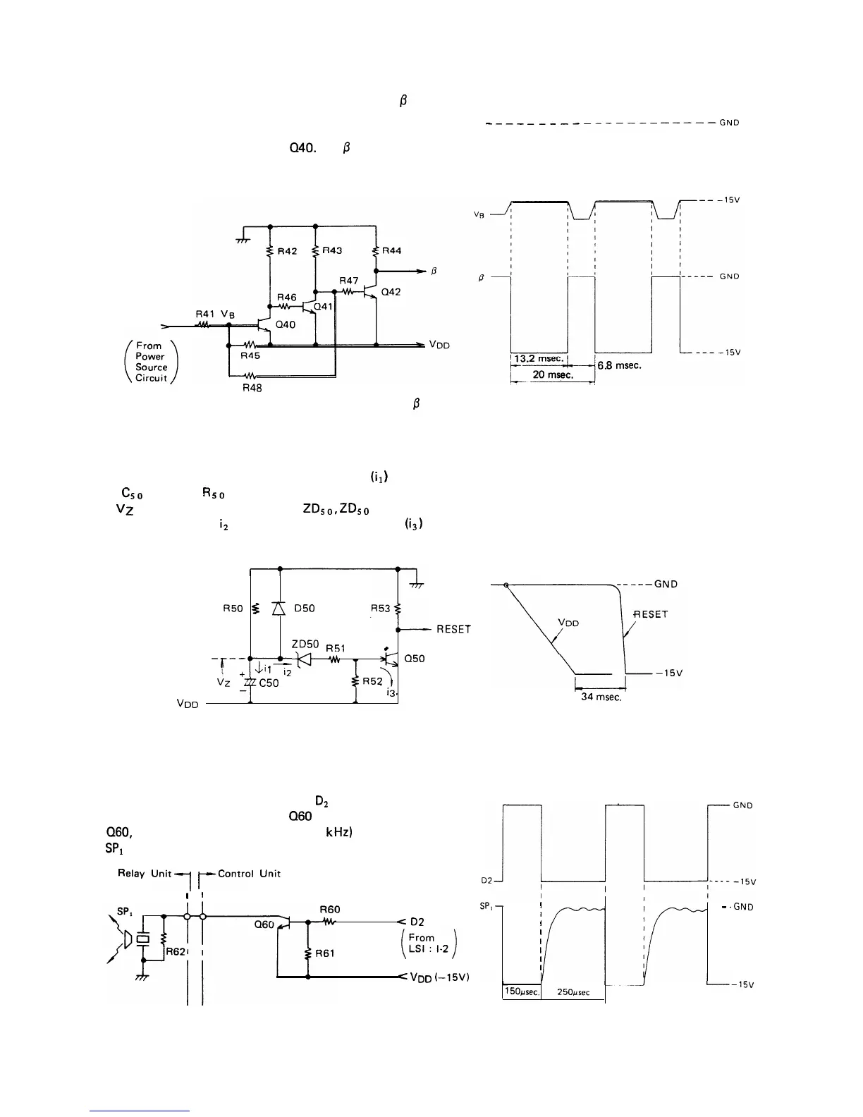
Half-wave rectified voltage (VB) from the power source
circuit is applied to the base of
Q40.
The
p
waveform is
generated from the collector of Q42.
This is the basic timing for all time processing.
-----___-
_-----_
--------ND
R48
Figure 20.
fl
Circuit and Waveform
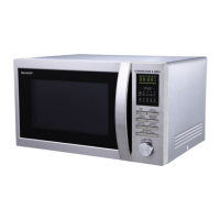
ACL CIRCUIT
By switching on power supply charge current
(iI
)
is fed
to
Cso
through
R
so
and generates Zener voltage (Vz).
If
Vz
exceeds the zener voltage of
ZDSO,
ZD5
o
is turned
on and the current
iz
flows. Thus the base current
(i3
)
flows through the transistor Q50 to turn on 050. By the
turning on of 050, a reset signal is obtained from the
collector.
R50
::
zx
D50
RESET
ZD50
R51
t
-[-J”&iJ’;;
w
3&
050
v*
c50
\
R52
i3.
VDD
34
msec.
Figure 21. ACL Circuit
BUZZER CIRCUIT
The square waveform developed from
D2
terminal of LSI
(l-2) is applied to the base of
060
to turn on and off
Q60, and squard waveform voltage (2.5 kHz) is applied to
SPI
to generate buzzer sound.
Relay
Unit1
rControl
Unit
I
1
R60
-=
02
<
VDD
(-15v)
sp,
-
I
--
-
.GND
I
I
I
I
I
I
I
--15v
15Opsec.
250usec
Figure 22. Buzzer Circuit
76