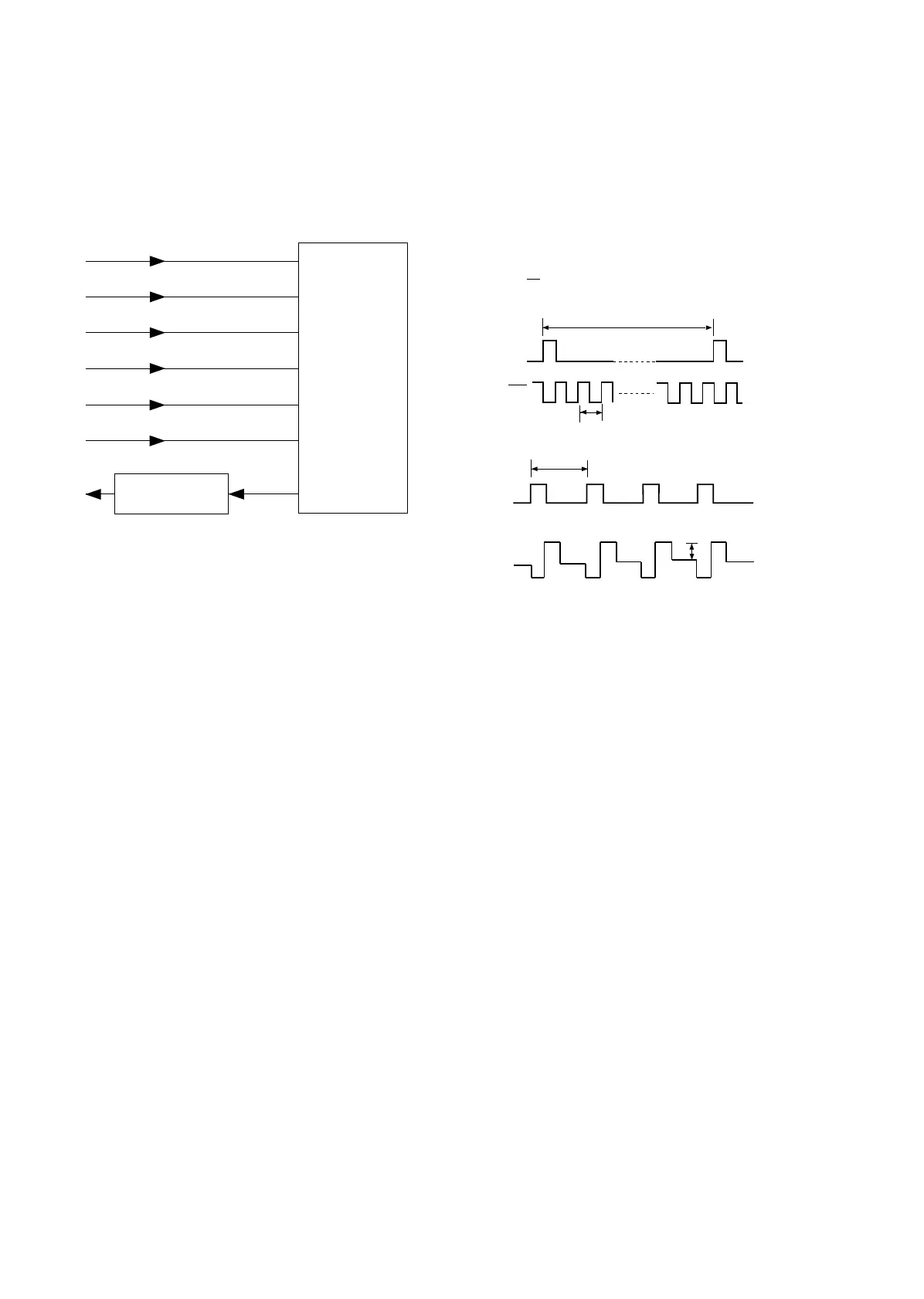
[5] Circuit description of CCD PWB
The CCD board picks up optical information from the document, con-
verts it into an electrical (analog) signal and transfers it to the control
boad.
(1) Block diagram
Fig. 8
(2) Description of blocks
1. CCD
The TCD1208P is a highly sensitive charged coupled image sensor
that consists of 2160 picture elements.
Receiving four drive signal (φT, φ2, φ1, φR) from the control board, the
tranferred photoelectric analog signal OS is impedance converted,
and the signal VO, is supplied to the control board.
2. Waveforms
1. φ1, φ2 (=φ1) signals within the control board.
Fig. 9
ΦT
Φ1
Φ2
+5V
GND
ΦR
VO
OUTPUT CIRCUIT
(emitter follower)
OS
CCD
TCD1208P
Approx. 5V
0V
Approx. 5V
0V
Approx. 5V
0V
Approx. 100mV
OS
φR
φ1 (=φ2)
φT
1.67µ Sec
5m Sec
1.67µ Sec
2. OS φ
UX-177H
5 – 11