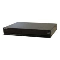
HBD-E2100/E3100/E3200/E4100/E6100
65
Pin No. Pin Name I/O Description
P43 FEGIO0 I/O
LDD serial interface data. The pin is spike-free at power-on stage.
The pin is not allowed to pull-up in circuit layout.
General IO
P44 FEGIO1 I/O PC RS232 serial receive data. The pin is spike-free at power-on stage.
P45 FEGIO5 O General IO
P46 DVCC33_IO_2 - 3.3V Digital IO Power
P47 FEGIO7 I/O
General IO. The pin is spike-free at power-on stage. The pin is not allowed to pull-up in
circuit layout.
P48 FEGIO6 O
Read gain switch 6. The pin is not allowed to pull-up in circuit layout.
General IO
P49 FEGIO4 O
Read gain switch 4
General IO
P50 FEGIO9 I/O
General IO. The pin is spike-free at power-on stage.
General IO
P51 FEGIO10 I/O PC RS232 serial receive data. The pin is spike-free at power-on stage.
P52 FEGIO11 I/O PC RS232 serial transmit data. The pin is spike-free at power-on stage.
P53 FETRAYIN_ I A logical Low indicates the Tray is IN
P54 FEGIO3 I/O
LED Control Output. Initial 0 Output. The pin is spike-free at power-on stage.
General IO
P55 USB_DM_P1 I/O USB port1 differential serial data bus (minus)
P56 USB_DP_P1 I/O USB port1 differential serial data bus (plus)
P57 USB_VRT_P1 - USB port1 reference resistor
P58 AVDD33_USB_P1 - 3.3V Analog power for USB port1
P59 EFPWRQ - 2.5 V power for E-fuse programming
P60 DVCC12_K_3 - 1.2V Digital Power
P61 DVCC33_IO_3 - 3.3V Digital IO Power
P62 SCL I USB over current Protection indication
P63 SDA I USB PCONT
P64 SPDIF_IN1 I HDMI ARC SPDIF input
P65 NFD0 I/O NAND Flash Data input/output bit0
P66 NFD1 I/O NAND Flash Data input/output bit1
P67 NFD2 I/O NAND Flash Data input/output bit2
P68 NFD3 I/O NAND Flash Data input/output bit3
P69 NFD4 I/O NAND Flash Data input/output bit4
P70 NFD5 I/O NAND Flash Data input/output bit5
P71 NFD6 I/O NAND Flash Data input/output bit6
P72 DVCC33_IO_4 - 3.3V Digital IO Power
P73 NFD7 I/O NAND Flash Data input/output bit7
P74 NFRBN I/O NAND Flash ready / busy
P75 NFREN I/O NAND Flash read enable
P76 NFCEN I/O NAND Flash chip enable
P77 NFCLE I/O NAND Flash command latch enable
P78 NFALE I/O NAND Flash address latch enable
P79 NFWEN I/O NAND Flash write enable
P80 DVCC12_K_4 - 1.2V Digital Power
P81 DDRVCCK_1 - 1.2V Digital Power
P82 RDQ4 I/O Memory data bit 4
P83 RDQ6 I/O Memory data bit 6
P84 RDQ2 I/O Memory data bit 2
P85 DDRVCCIO_1 - 1.5V Digital IO Power
P86 RDQ0 I/O Memory data bit 0
P87 RDQ11 I/O Memory data bit 11
P88 RDQ9 I/O Memory data bit 9
P89 RDQ13 I/O Memory data bit 13
P90 RDQ15 I/O Memory data bit 15
Ver. 1.5