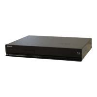
HBD-E2100/E3100/E3200/E4100/E6100
74
MB1002 BOARD (6/6) IC801 R5F3650KCDFB
(SYSTEM CONTROLLER)
Pin No. Pin Name I/O Description
1 SIRCS_IN I SIRCS signal input from the remote control receiver
2 FAN_CONT O
Fan motor speed control signal output terminal control by DA converter
Port output higher, speed slower
3 FL_DOUT O Serial data output to the fl uorescent indicator tube driver
4 NO_USE - No used
5 FL_CLK O Serial data transfer clock signal output to the fl uorescent indicator tube driver
6 BYTE I External data bus width selection signal input terminal
7 CNVSS I Processor mode selection signal input terminal
8 NFC_SW O Stand-by control signal output to the NFC module
9 NFC_IRQ I Wireless data reception signal input from NFC module
10 RESET I
System reset signal input from the reset signal generator and reset switch "L": reset
For several hundreds msec. After the power supply rises, "L" is input, then it change to
"H"
11 XOUT O System clock output terminal (8MHz)
12 VSS - Ground terminal
13 XIN I System clock input terminal (5MHz)
14 VCC1 - Power supply terminal (+3.3V)
15 CEC_TX_RX I/O CEC serial data input/output with the HDMI connector
16 NO_USE - No used
17 NO_USE - No used
18 AC_CUT I AC cut detection signal input terminal "L": AC cut
19 NO_USE - No used
20 NO_USE - No used
21 NO_USE - No used
22 NO_USE - No used
23 NO_USE - No used
24 WHITE_LED O Front panel LED drive signal output terminal “H”: on
25 PCONT_FL O
Power supply on/off control signal output terminal for fl uorescent indicator tube driver
"H": power on
26 BT_LED O Bluetooth LED drive signal output terminal “H”: on
27 NO_USE - No used
28 NO_USE - No used
29 TXD1 O TXD1 (for debug) / fl ash write TXD1
30 RXD1 I RXD2 (for debug) / fl ash write RXD1
31 ON CHIP DEBUG / CLK1 I On chip debuger / fl ash write CLK1
32 NO_USE / RTS1 O No used
33 TAS5538_SDA I/O Two-way data bus with the DAMP processor
34 TAS5538_SCL I/O Serial data transfer clock signal output to the DAMP processor
35 DC_DET I Speaker DC detection signal input terminal "L": speaker DC is detected
36 PCONT1 O Power supply on/off control signal output terminal "H": power on
37 PCONT2 O Power supply on/off control signal output terminal “H”: power on
38 PCONT3 O Power supply on/off control signal output terminal "H": power on
39 EPM O EPM for update used
40 PCONT_STA516 O STA516 IC Power Control, "H": power on
41 NO_USE - No used
42 FAN_ON O Power supply on/off control signal output terminal for fan motor "H": power on
43 NO_USE - No used
44 CE I Chip enable signal input terminal
45 ST_SDA I/O Two-way data bus with the FM receiver
46 ST_SCL I/O Serial data transfer clock signal output to the FM receiver
47 BD_IF_START O Ready signal output to the BD decoder "H": ready
48 TAS5538_XPDN O Power down signal output to the power amplifi er "L": power down
49 BD_IF_REQ I Request signal input from the BD decoder “H”: request
Ver. 1.5