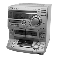
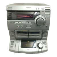
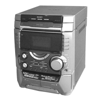
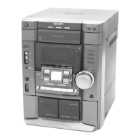
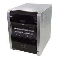
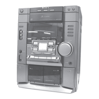
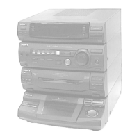
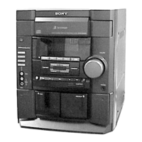
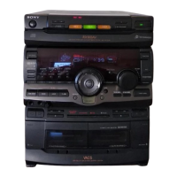
HCD-DR8AV/W900AV
— 35 — — 36 —
THIS NOTE IS COMMON FOR PRINTED WIRING
BOARDS AND SCHEMATIC DIAGRAMS.
(In addition to this, the necessary note is printed
in each block.)
For schematic diagrams.
Note:
• All capacitors are in µF unless otherwise noted. pF: µµF
50 WV or less are not indicated except for electrolytics
and tantalums.
• All resistors are in Ω and
1
/
4
W or less unless otherwise
specified.
•
¢
: internal component.
• C : panel designation.
For printed wiring boards.
Note:
• X : parts extracted from the component side.
•
®
: Through hole.
•
¢
: internal component.
• b : Pattern from the side which enables seeing.
(The other layers' patterns are not indicated.)
• U : B+ Line.
• V : B– Line.
• H : adjustment for repair.
• Voltages and waveforms are dc with respect to ground
under no-signal (detuned) conditions.
• Voltages are taken with a VOM (Input impedance 10 MΩ).
Voltage variations may be noted due to normal produc-
tion tolerances.
• Waveforms are taken with a oscilloscope.
Voltage variations may be noted due to normal produc-
tion tolerances.
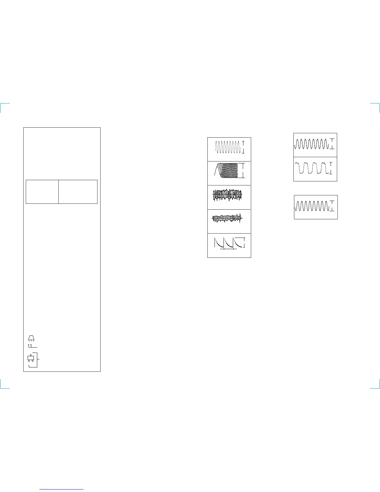
• Circled numbers refer to waveforms.
• Signal path.
F : FM
g : VIDEO/MD
E : PB (DECK A)
d : PB (DECK B)
G : REC (DECK B)
J : CD
c : digital out
I : PHONO
• Abbreviation
CND : Canadian model
AUS : Australian model
EA : Saudi Arabia model
MX : Mexican model
SP : Singapore model
AR : Argentina model
IC101 #ª FE
1
2
3
4
5
Waveforms
– BD SECTION –
IC101 ^¶ XTAI
IC101 %¡ RF AC
IC101 $¡ TE
IC101 @§ MDP
• Indication of transistor
C
These are omitted
EB
Q
C
These are omitted
EB
1
IC601 &™ X-OUT
– FL Section –
1
2
IC501 !¡ XC-OUT
IC501 !£ X-OUT
– MAIN (2/5) Section –
3.1Vp-p
16.9MHz
1.2Vp-p
(PLAY)
2.5V
APPROX 500mVp-p
7.5µsec
2.4Vp-p
16MHz
5.5Vp-p
32.768kHz
5.2Vp-p
12.5MHz
3.4Vp-p
Note:
The components identi-
fied by mark ! or dotted
line with mark ! are criti-
cal for safety.
Replace only with part
number specified.
Note:
Les composants identifiés par
une marque ! sont critiques
pour la sécurité.
Ne les remplacer que par une
piéce portant le numéro
spécifié.