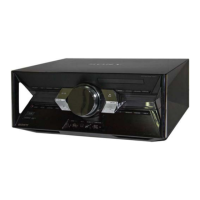
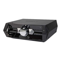
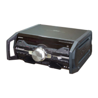
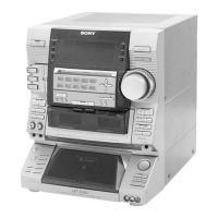
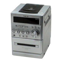
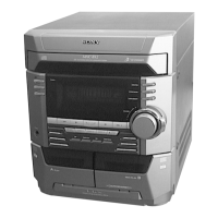
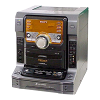
HCD-SHAKE7
HCD-SHAKE7
2727
Note on Schematic Diagram:
• All capacitors are in μF unless otherwise noted. (p: pF)
50 WV or less are not indicated except for electrolytics
and tantalums.
• All resistors are in and
1
/4 W or less unless otherwise
specifi ed.
•
2
: nonfl ammable resistor.
• C : panel designation.
• Note for Printed Wiring Boards and Schematic Diagrams
• A : B+ Line.
• B : B– Line.
• Voltage and waveforms are dc with respect to ground
under no-signal (detuned) conditions.
no mark : TUNER
< > : CD PLAY
*
: Impossible to measure
• Voltages are taken with a VOM (Input impedance 10 MΩ).
Voltage variations may be noted due to normal production
tolerances.
• Waveforms are taken with a oscilloscope.
Voltage variations may be noted due to normal production
tolerances.
• Circled numbers refer to waveforms.
• Signal path.
F : AUDIO
f : TUNER (FM/AM)
N : MIC
J : CD PLAY
E : USB
• Abbreviation
AR : Argentina
model
E2 : 120 V AC area in E model
E4 : African model
E51 : Chilean and Peruvian models
EA : Saudi Arabia model
MX : Mexican model
MY : Malaysia model
SAF : South African model
Note on Printed Wiring Board:
• X : parts extracted from the component side.
• : parts extracted from the conductor side.
•
: Pattern from the side which enables seeing.
(The other layer’s patterns are not indicated.)
Caution:
Pattern face side:
(Conductor Side)
Parts face side:
(Component Side)
Parts on the pattern face side seen from
the pattern face are indicated.
Parts on the parts face side seen from
the parts face are indicated.
Note: The components identifi ed by mark 0 or
dotted line with mark 0 are critical for safety.
Replace only with part number specifi ed.
• Abbreviation
AR : Argentina model
E2 : 120 V AC area in E model
E4 : African model
E51 : Chilean and Peruvian models
EA : Saudi Arabia model
MX : Mexican model
MY : Malaysia model
SAF : South African model
C
B
These are omitted.
E
Q
t Indication of transistor
D
G
These are omitted.
S
Q
B
These are omitted.
CE
Q
B
These are omitted.
CE
Q
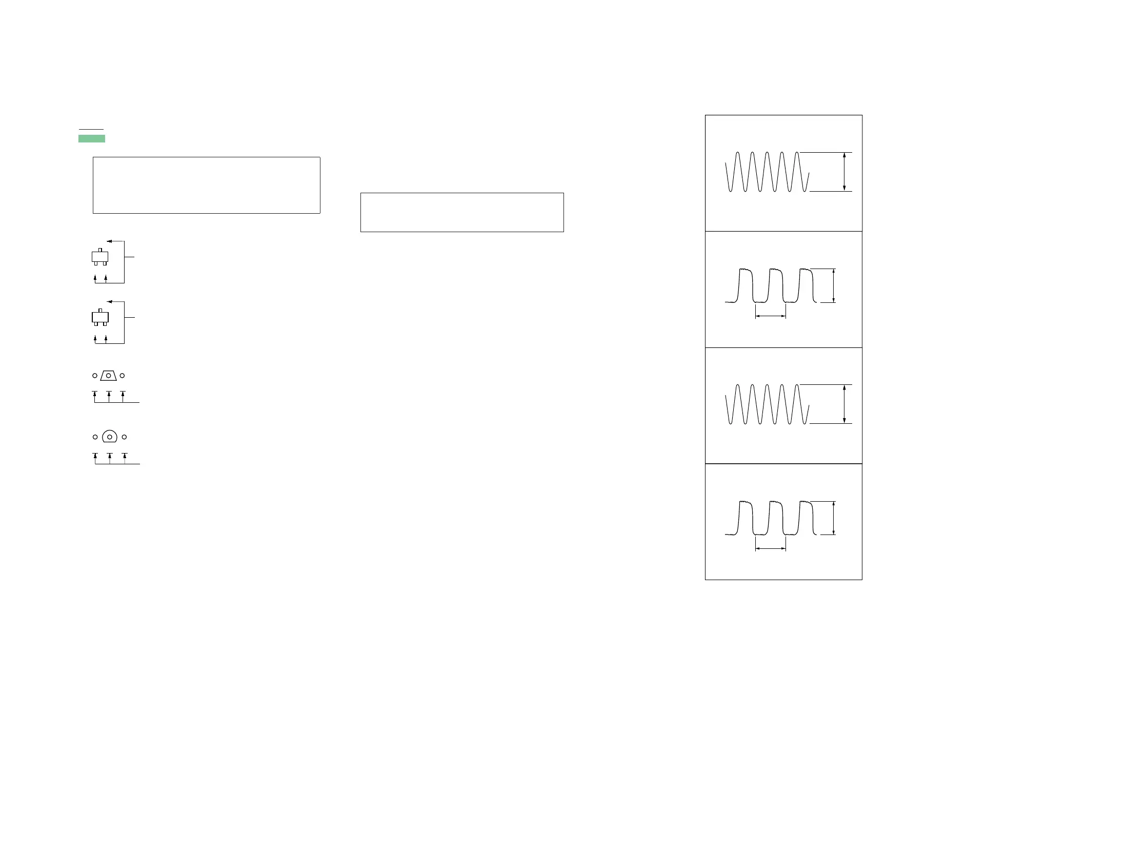
• Waveforms
– MOTHERBOARD Board –
120 mVp-p
24.0 MHz
1 IC9 es (XTAL2)
20 mV/DIV, 10 ns/DIV
236 mVp-p
8.0 MHz
3 IC11 qd (I-Xin)
50 mV/DIV, 50 ns/DIV
4 IC656 4 (XTALO)
50 mV/DIV, 25 ns/DIV
12.28 MHz
198 mVp-p
2 IC11 8 (I-X-CIN)
20 mV/DIV, 10 Ps/DIV
32.76 MHz
75.2 mVp-p
Ver. 1.2