MHC-V42D
MHC-V42D
3838
Caution:
Pattern face side:
(Conductor Side)
Parts face side:
(Component Side)
Parts on the pattern face side seen from
the pattern face are indicated.
Parts on the parts face side seen from
the parts face are indicated.
Note on Schematic Diagram:
• AllcapacitorsareinµFunlessotherwisenoted.(p:pF)
50 V or less are not indicated except for electrolytics
and tantalums.
• AllresistorsareinΩ and
1
/4 W or less unless otherwise
specied.
• f : Internal component.
•
2
:Nonammableresistor.
•
5
:Fusibleresistor.
• C : Panel designation.
• Note for Printed Wiring Boards and Schematic Diagrams
• A : B+ Line.
• B : B– Line.
• H : Adjustment for repair.
• Voltageandwaveformsaredcwithrespecttoground
under no-signal (detuned) conditions.
no mark: TUNER
( ): CD PLAY
{ }: DVD PLAY
[ ]: USB
< >: Bluetooth
*:Impossibletomeasure
• VoltagesaretakenwithaVOM(Inputimpedance10MΩ).
Voltagevariationsmaybenotedduetonormalproduction
tolerances.
• Waveformsaretakenwithaoscilloscope.
Voltagevariationsmaybenotedduetonormalproduction
tolerances.
• Circlednumbersrefertowaveforms.
• Signalpath.
c : DVD PLAY
J : AUDIO (DIGITAL)
F : AUDIO (ANALOG)
N : MIC
f : TUNER (FM)
a : BLUETOOTH
L : VIDEO
E : USB
Note on Printed Wiring Board:
• X : parts extracted from the component side.
• :partsextractedfromtheconductorside.
•
:Patternfromthesidewhichenablesseeing.
(The other layer’s patterns are not indicated.)
C
B
These are omitted.
E
Q
• Indication of transistor.
D
G
These are omitted.
S
Q
B
These are omitted.
C E
Q
B
These are omitted.
C E
Q
Note 2: When the MS-476boardis defective,exchange
the entire CDM90 ASSY.
Note 3: When the MOTHERBOARD mounted pc board
is replaced, be sure to refer to “DESTINATION
SETTING METHOD” on page 5.
Note 1: W h e n t h e M O T H E R B O A R D b o a r d i s
replaced, spread the compound referring to
“ NOTE O F R E P L A C I NG T H E I C 2 0 0 2 O N
T H E M O T H E R B O A R D B O A R D A N D T H E
MOTHERBOARD MOUNTED PC BOARD” on
servicing notes (page 6).
Note: The components identied by mark 0 or
dotted line with mark 0 are critical for safety.
Replaceonlywithpartnumberspecied.
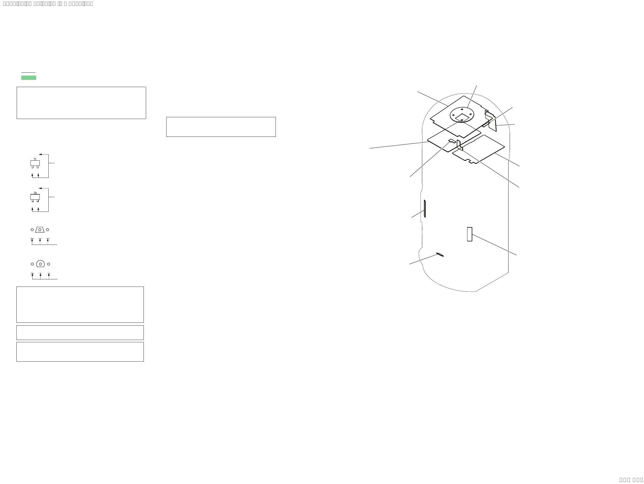
• Circuit Boards Location
• MOTHERBOARDboardismultilayerprintedboard.
However, the patterns of intermediate layers have not
beenincludedindiagrams.
PANEL board
(EXCEPT MY, E12),
PANEL (PANA) board
(MY, E12)
GESTURE board
MIC board
(AR, TH, E12, LA9),
MIC (EMC) board
(AEP, UK, RU, MY, AUS, E4, E93)
NFC board
MOTHERBOARD board
SMPS board
(AR, TH, E12, LA9),
SMPS (EMC) board
(AEP, UK, RU, MY, AUS, E4, E93)
FL PARTY board
FR PARTY board
SW LED board
IR board
MS-476 board
SYSSET
2019/03/0500:47:46(GMT+09:00)
 Loading...