5-4
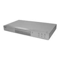
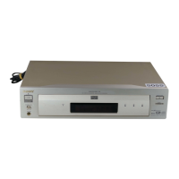
DVP-NS975V
Pin No. Pin name Type Function
150 RA2 Output DRAM address bit2
151 RA3 Output DRAM address bit3
152 DVDD18 Power 1.8V power pin for internal digital circuitry
153 RVREF Analog Input Reference voltage for DDR DRAM
154 RCLKB Output DRAM clock invert
155 DVDD3 Power 3.3V power pin for internal digital circuitry
156 DRCLK Output DRAM clock
157 CKE Output DRAM clock enable
158 RA11 Output PD DRAM address bit11
159 RA9 Output DRAM address bit9
160 RA8 Output DRAM address bit8
161 DVSS Ground Ground pin for internal digital circuitry
162 RA7 Output DRAM address bit7
163 DVSS Ground Ground pin for internal digital circuitry
164 RA6 Output DRAM address bit6
165 RA5 Output DRAM address bit5
166 RA4 Output DRAM address bit4
167 DVDD3 Power 3.3V power pin for internal digital circuitry
Output PU
168 DISC/xEXT Default Low DISC/External input select output signal (H: DISC, L: EXTin)
169 RGBSEL Output PU RGB/YCbCr select output signal (H: RGB Disable, L: RGB Enable)
Output Default
170 xsmrst Low Reset output signal for HDMI sub CPU (Low Active)
171 WIDE Output Voltage select output signal for S terminal (H: 16:9, L: 4:3)
Output Default
172 NT/xPAL Low NTSC/PAL select output signal (H: NTSC, L: PAL)
173 DVDD18 Power 1.8V power pin for internal digital circuitry
Output Default
174 EUROVY High CVBS/S terminal select output signal (H:CBVS, L: S-terminal)
175 DVSS Ground Ground pin for internal digital circuitry
176 LIMITSW Input GPIO bit9 for Servo group
177 OCSW Input GPIO bit8 for Servo group
Output PU
178 VCLK Default Low 27MHz synchoronous clock output for Video data
179 CKSW Input PU GPIO bit7 for Servo group
180 IO3 Output PD GPIO
181 TSD_M Output PD GPIO bit5 for Servo group
182 DVDD3 Power 3.3V power pin for internal digital circuitry
183 MUTE Output PD GPIO bit4 for Servo group
184 MUTE123 Output PD GPIO bit3 for Servo group
185 REV Output PD GPIO bit2 for Servo group
186 FWD Output PD GPIO bit1 for Servo group
187 MSW Input PD GPIO bit0 for Servo group
188 DSEL Output PD Interlace/Progressive select output signal (H: 480p, L: 480i)
189 DACVDDC Power 3.3V power for Video DAC circuitry
190 VREF Analog Input Bandgap Ref Voltage (No connect)
191 FS Analog Input Full Scale Adjustment
Compensation capacitor
192 CIN/YUV0 Output Video data output bit0
193 DACVDDC Ground Ground pin for Video DAC circuitry
Analog Y output
194 Y/YUV1 Output Video data output bit1
195 DACVDDB Power 3.3V power for Video DAC circuitry
Analog chroma output
196 C/YUV2 Output Video data output bit2
w
w
w
.
x
i
a
o
y
u
1
6
3
.
c
o
m
Q
Q
3
7
6
3
1
5
1
5
0
9
9
2
8
9
4
2
9
8
T
E
L
1
3
9
4
2
2
9
6
5
1
3
9
9
2
8
9
4
2
9
8
0
5
1
5
1
3
6
7
3
Q
Q
TEL 13942296513 QQ 376315150 892498299
TEL 13942296513 QQ 376315150 892498299
http://www.xiaoyu163.com
http://www.xiaoyu163.com