SORENSEN DCS SERIES MANUAL THEORY OF OPERATION
3-1
SECTION 3. THEORY OF OPERATION
3.1 Power Circuit (A2 Assembly)
This section describes the operation of the A2 assembly switching regulator power circuit. Three subsections cover
basic switching regulator theory, a simplified description of the Sorensen full bridge converter, and a more detailed
circuit description intended for troubleshooting purposes.
3.1.1 Basic Off-Line Switching Regulator Theory
An off-line switching power supply first converts the AC input line voltage to high voltage DC by diode
rectification and then chops the DC at a high frequency. This high frequency waveform is applied to the primary
of a power transformer which provides a step-up or step-down in voltage and electrical isolation on its secondary.
The secondary waveform is rectified and filtered, giving a smooth DC output voltage. Feedback from the
secondary circuit is applied to a pulse width modulator (PWM) control circuit which controls the on-time of the
primary circuit switching waveform. This increases or decreases the voltage on the secondary of the power
transformer so that output regulation is obtained.
The use of high frequency transformers in switching power supplies has the advantage of requiring less volume,
less weight, and dissipating less heat than the lower frequency transformers in conventional linear power supplies.
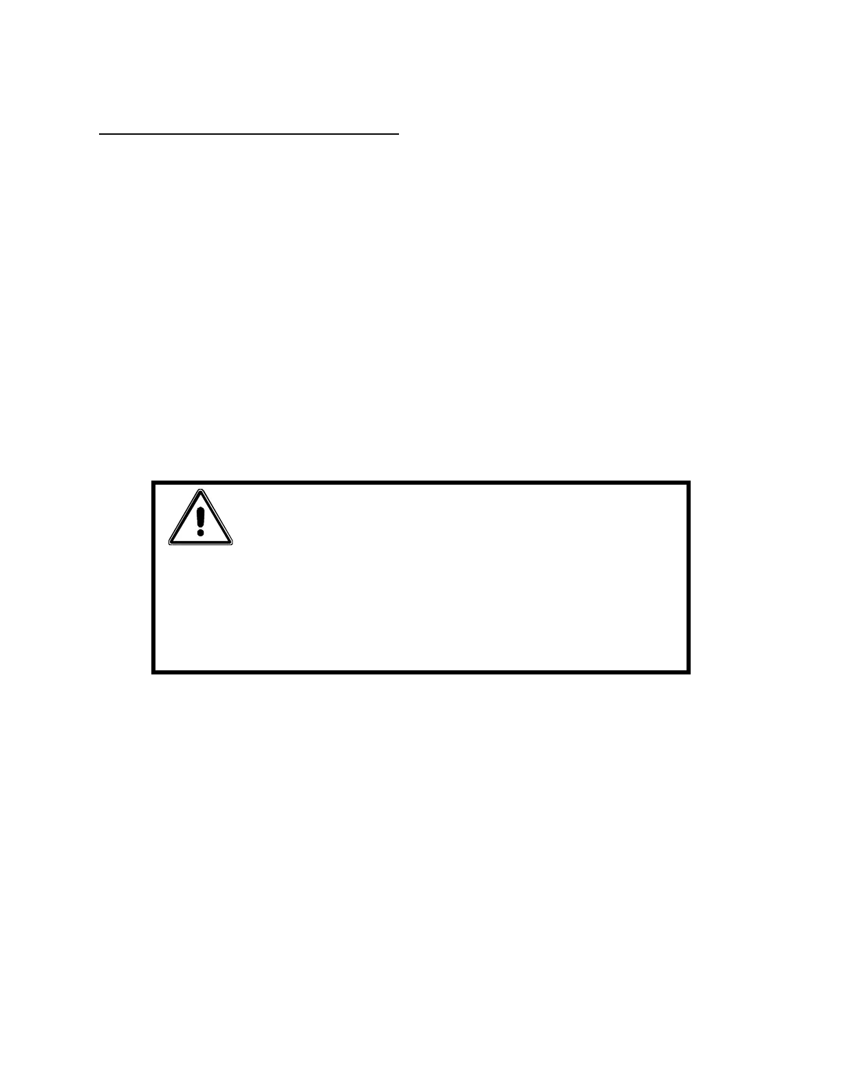
CAUTION!
Potentially LETHAL VOLTAGES exist on the A2 circuit board on the primary
side of the isolation barrier. Troubleshoot with care, preferably with power off and
recognizing that filter capacitors store potentially LETHAL and DESTRUCTIVE
ENERGY even for some time AFTER POWER is REMOVED. Always use an
isolation transformer connected ONLY to the power supply input when making test
measurements on the primary side circuits.
3.1.2 Simplified Full Bridge Converter Theory
See Figure 3-1.
The input AC line voltage is rectified and filtered by CR35, C32(A,B,C), and C72(A,B,C) to a raw DC voltage
which is supplied to the power FETs Q13-Q16 on the primary of power transformer T1. Resistor R116 and relay
K1 form an input surge current limiter which reduces the inrush current to the filter capacitors C32(A,B,C), and
C72(A,B,C) during power-up. The power FETs and the primary winding of T1 form a bridge which is driven at
70 kHz by pulse width modulator (PWM) U6 through FETs Q7-Q12, Q18 and Q19 and drive transformer T2. A
current sense transformer T3 in the primary of the power transformer provides a feedback signal to the PWM
which is compared to a limited error signal derived from the output current and voltage control circuits. The
output of the comparator controls the on time of the PWM output drive waveforms on a cycle by cycle basis thereby
controlling the primary current and the output of the power transformer. Diodes CR301 and CR302
(CR301-CR304 on models DCS 150-7 and 300-3.5 and CR300-CR307 on model DCS 600-1.7) rectify the output
of power transformer T1 and inductor L3 and capacitors C51, C52 and C53 filter the rectified signal to provide the
DC output.
www.valuetronics.com