SORENSEN DCS SERIES MANUAL THEORY OF OPERATION
3-3
A current shunt (R91) in the output return line develops a voltage dependent on the output current. This current
information is compared to the setting of the front panel current limit control in the current control circuit (U4-1
and U15). The output voltage is also monitored and compared to the front panel voltage control setting in the
voltage control circuit (U5). The outputs of the voltage and current control circuits are OR’d and this signal is fed
into the PWM error amplifier inverting input providing the negative feedback required to produce a regulated
output. The output voltage and current information from the current and voltage control circuits is also fed to the
front panel A1 assembly where it is displayed on the digital voltage and current readouts.
Transformer T4, rectifier CR42 and regulators U9-U13 provide the necessary auxiliary supply voltages for the
PWM circuit, the voltage and current control circuits, the A1 metering board and the raw DC supply for drive
transformer T2. A 6.2 volt reference is also derived from the 12V supply for use in metering circuits by diode CR1
and resistor R2.
Transformers T1, T3 and T4 provide output isolation from the line potentials in the primary circuit, the PWM
circuit and the auxiliary supply circuits respectively.
3.1.3 Detailed Circuit Description
This section is intended to provide further detail for troubleshooting purposes. Please read the previous section as
an overview and then refer to the detailed assembly schematic in Section 6.
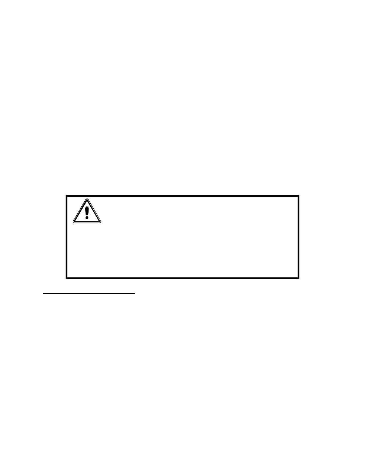
CAUTION!
Potentially LETHAL VOLTAGES exist on the A2 circuit board on the primary
side of the isolation barrier. Troubleshoot with care, preferably with power off and
recognizing that filter capacitors store potentially LETHAL and DESTRUCTIVE
ENERGY even for some time AFTER POWER is REMOVED. Always use an
isolation transformer connected ONLY to the power supply input when making test
measurements on the primary side circuits.
Input Rectifier and Inrush Limiting
Input ac power passes from the rear panel ac connector (TB1) through an RFI filter consisting of C1-6, R122, L1,
and L2 to the front panel power switch. Both input lines are switched with one line (the neutral line of a 115Vac
input) returning to the A2 PCB and the input rectifier CR35 via fuse F1. The other input line (the hot line of a
115Vac input) is connected to the remaining input of rectifier CR35 via front panel circuit breaker CB1, fuse F2
and the inrush limiter formed by resistor R116 and relay K1. Resistor R116 limits the power-on inrush current to
the main filter capacitors C32(A,B,C) and C72(A,B,C) until it is shorted by K1 relay contacts. The time delay for
K1 contact closure is determined by the time constant formed by capacitor C12, resistor R118 and the gate
threshold of FET Q6. Diode CR38 discharges C12 when the 12V auxiliary supply collapses and CR39 provides an
inductive kickback path for the relay coil. During the inrush period diode CR33 holds the PWM shutdown line
high, disabling the power supply output until Q6 turns on. Resistors R114 and R115 are bleeder resistors for the
main filter capacitors. The rectified high voltage dc from CR35 is supplied to the main switching FETs Q13-Q16
on the primary of the power transformer T1 via fuse F3.
www.valuetronics.com