BIOS Setup Utility
SY-7VBA133U
62
After you have completed the changes, press [Esc] and follow the
instructions on your screen to save your settings or exit without saving.
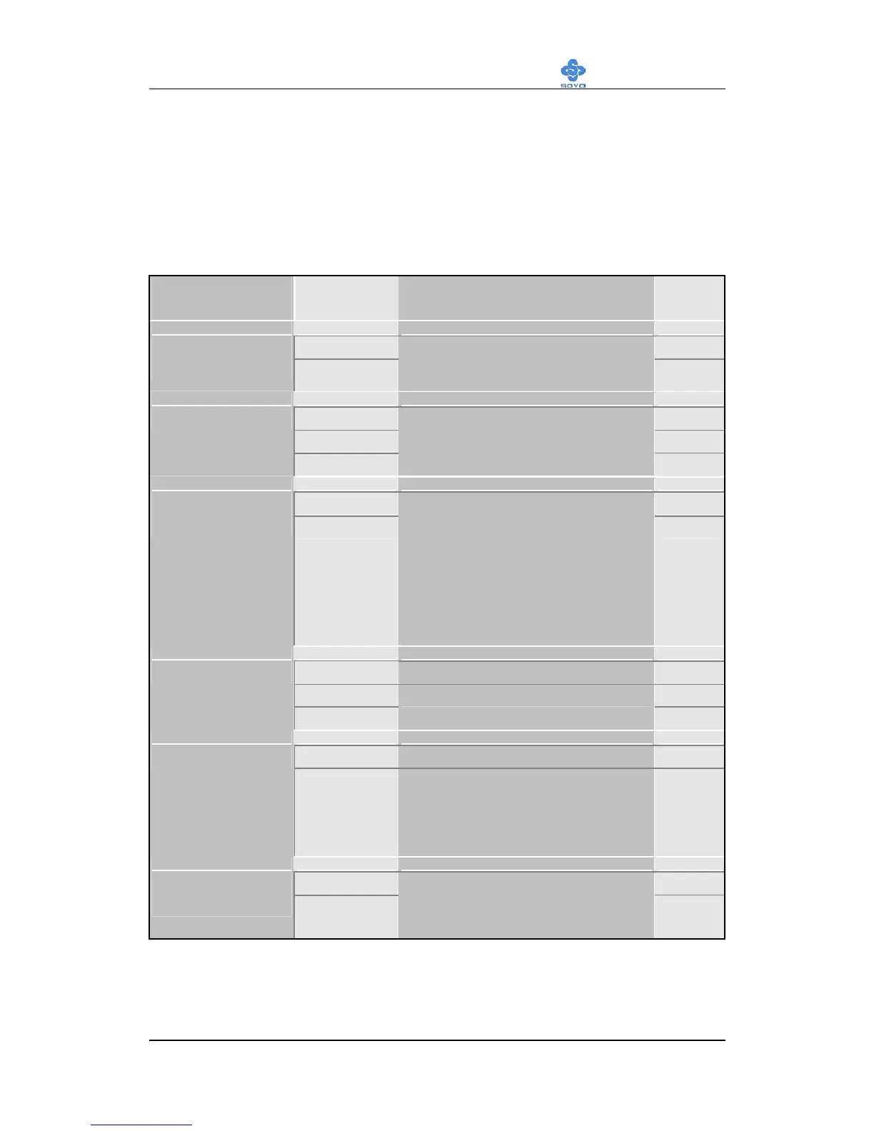
The following table describes each field in the Advanced Chipset Features
Menu and how to configure each parameter.
3-4.1 CHIPSET FEATURES SETUP
CHIPSET
FEATURES
Setting Description Note
Disable
DRAM Timing
By SPD
Enabled
If enable the DRAM will auto
detect the DRAM timing.
Default
Host Clock Default
HCLK-33M
DRAM Clock
HCLK+33M
This item allows you to control
the DRAM speed.
2
SDRAM Cycle
Length
3
When synchronous DRAM is
installed, the number of clock
cycles of CAS latency depends
on the DRAM timing. Do not
reset this field from the default
value specified by the system
designer.
Default
4 Bank Increase DRAM performance.
Disabled Default
Bank Interleave
2 Bank
Disabled Default
Memory Hole
Enabled Some interface cards will map
their ROM address to this area.
If this occurs, select [Enabled] in
this field.
Disabled
P2C/C2P
Concurrency
Enabled
This item allows you to
enable/disable the PCI to CPU,
CPU to PCI concurrency
Default

 Loading...