Single and Multichannel Detector (SCD) / (MCD)
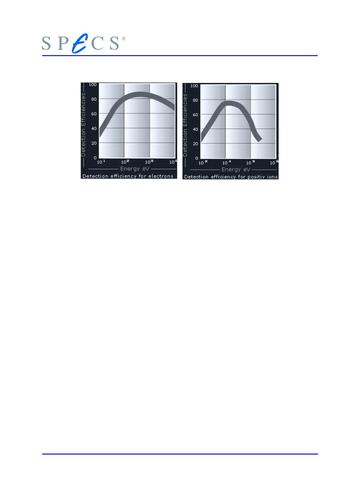
Figure 19: Detection Efficiency for Electrons and Ions
The BIAS voltage produced in the HSA3500 determines the conversion energy
(23)
of the charged particles impinging on the CEM. The proper conversion voltage has two
requirements which must be simultaneously fulfilled:
● the particles energy should be suitable for maximum yield of secondary electron
emission at the impact on the CEM wall. For electrons this is roughly in the en-
ergy range between 100 - 800 eV.
● For ions, the yield increases with the kinetic energy roughly up to 10 keV.
Standard settings are:
● for electrons: U
BIAS
= + 90 V.
● for ions: U
BIAS
= - 2000 V.
3.5.5 Spectrometer Voltage U
0
The main retardation voltage of the spectrometer U0 is numerically equal to the differ-
ence between kinetic energy (Ekin) and pass energy (Epass) + Work Function (WF). Be-
cause of the different polarity of the lens and hemisphere voltages in the different ana-
lyzer modes (XPS,AES,UPS or ISS) the value U0 is calculated by
U
groundplate
=
E
kin
−
E
pass
−
WF
/
q
(24)
The spectrometer voltage is applied on a groundplate and lens element 10 (Figure 5:
Analyzer Main Components and Voltage Principle page 10 and Figure 33: Schematics of
the 12-pin Analyzer Feedthrough page 72 as well as the comments in section , "" on
page .
Example:
WF=4.5 eV, Ekin =1000 eV, Ep= 100V
PHOIBOS 33
 Loading...