Chapter
LF List of Figures
Figure 1: Package Contents........................................................................................................................6
Figure 2: Connection Scheme....................................................................................................................7
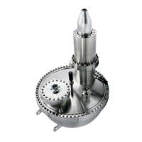
Figure 3: Analyzer Housing (PHOIBOS100)...............................................................................................8
Figure 4: Analyzer Housing (PHOIBOS150)...............................................................................................9
Figure 5: Analyzer Main Components and Voltage Principle................................................................10
Figure 6: High Point Transmission Mode.................................................................................................13
Figure 7: Medium Area Mode..................................................................................................................14
Figure 8: High Magnification Mode........................................................................................................15
Figure 9: Typical Intensity-Position Profile with Iris Aperture................................................................17
Figure 10: PHOIBOS µ-Metal Shielding...................................................................................................21
Figure 11: Magnetic Field of the Trim Coil..............................................................................................22
Figure 12: External Rotary Dial for Positioning......................................................................................24
Figure 13: Entrance and Exit Slit Rings (Slit Combination 4-B)..............................................................24
Figure 14: Exit Slit Selection.....................................................................................................................25
Figure 15: Detector Sweep, Count rate vs. Voltage................................................................................29
Figure 16: Lifetime of the Extended Dynamic Range CEM....................................................................30
Figure 17: Linearity Plot for the new Extended Range CEM..................................................................31
Figure 18: Efficiency Plot for the new Extended Range CEM................................................................32
Figure 19: Detection Efficiency for Electrons and Ions...........................................................................33
Figure 20: Energy Scheme – Photoelectron Spectroscopy......................................................................34
Figure 21: Removal of the Transportation Locks....................................................................................38
Figure 22: Corresponding Hole in the Ground Plate..............................................................................39
Figure 23: Mounting Tips.........................................................................................................................42
Figure 24: Detector Flange.......................................................................................................................43
Figure 25: Starting up the detector.........................................................................................................48
Figure 26: Menu - “Analyzer Settings”...................................................................................................58
Figure 27: Analyzer Cailbration Procedure.............................................................................................59
Figure 28: MCD Calibration......................................................................................................................60
Figure 29: Fermi Edge Operation ...........................................................................................................62
Figure 30: Fermi Edge Operation ...........................................................................................................63
Figure 31: XPS on Silver, Wide Scan (PHOIBOS 150 MCD9)....................................................................68
Figure 32: XPS on Silver, Ag 3d (PHOIBOS 150 MCD9)...........................................................................70
Figure 33: Schematics of the 12-pin Analyzer Feedthrough..................................................................72
Figure 34: Schematics of the 12 pin Detector Feedthrough...................................................................73
Figure 35: PCU Amplifier Test..................................................................................................................76
Figure 36: CounterChannelMask for MCD9, 1+2+8+9 off......................................................................78
Figure 37: Screws fixing the ceramic rods and adjustment crew...........................................................83
Figure 38: Pull back the Ceramic Rods, Remove the Channeltron.........................................................83
PHOIBOS I
 Loading...