Electrical characteristics L6470
12/64 Doc ID 16737 Rev 2
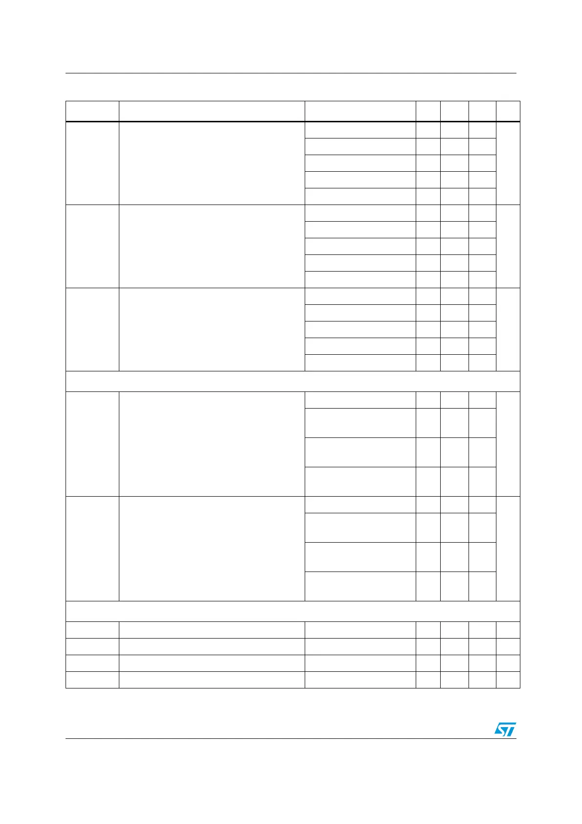
t
f
Fall time
(3)
POW_SR = '00'; Iout = +1A 90
ns
POW_SR = '00'; Iout = -1A 110
POW_SR = ‘11’, I
out
= ±1A 110
POW_SR = ‘10’, I
out
= ±1A 260
POW_SR = ‘01’, I
load
= ±1A 375
SR
out_r
Output rising slew-rate
POW_SR = '00', I
out
= +1A 285
V/µs
POW_SR = '00', I
out
= -1A 360
POW_SR = ‘11’, I
out
= ±1A 285
POW_SR = ‘10’, I
out
= ±1A 150
POW_SR = ‘01’, I
out
= ±1A 95
SR
out_f
Output falling slew-rate
POW_SR = '00', I
out
= +1A 320
V/µs
POW_SR = '00', I
out
= -1A 260
POW_SR = ‘11’, I
out
= ±1A 260
POW_SR = ‘10’, I
out
= ±1A 110
POW_SR = ‘01’, I
out
= ±1A 75
Dead time and blanking
t
DT
Dead time
POW_SR = '00' 250
ns
POW_SR = ‘11’,
f
OSC
= 16MHz
375
POW_SR = ‘10’,
f
OSC
= 16MHz
625
POW_SR = ‘01’,
f
OSC
= 16MHz
875
t
blank
Blanking time
POW_SR = '00' 250
ns
POW_SR = ‘11’,
f
OSC
= 16MHz
375
POW_SR = ‘10’,
f
OSC
= 16MHz
625
POW_SR = ‘01’,
f
OSC
= 16MHz
875
Source-drain diodes
V
SD,HS
High side diode forward ON voltage I
out
= 1 A 1 1.1 V
V
SD,LS
Low side diode forward ON voltage I
out
= 1 A 1 1.1 V
t
rrHS
High side diode reverse recovery time I
out
= 1 A 30 ns
t
rrLS
Low side diode reverse recovery time I
out
= 1 A 100 ns
Table 4. Electrical characteristics (continued)
Symbol Parameter Test condition Min Typ Max Unit
 Loading...