L6470 Electrical data
Doc ID 16737 Rev 2 9/64
2 Electrical data
2.1 Absolute maximum ratings
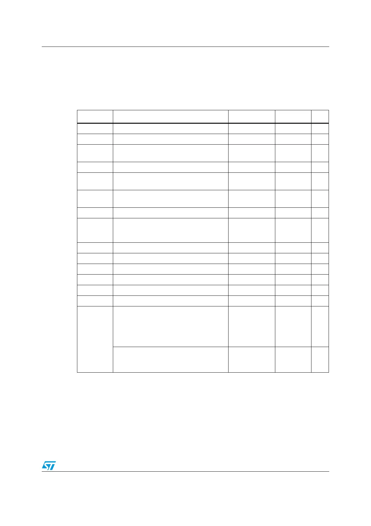
Table 2. Absolute maximum ratings
Symbol Parameter Test condition Value Unit
V
DD
Logic interface supply voltage 5.5 V
V
S
Motor supply voltage V
SA
= V
SB
= V
S
48 V
V
GND, diff
Differential voltage between AGND, PGND
and DGND
±0.3 V
V
boot
Bootstrap peak voltage 55 V
V
REG
Internal voltage regulator output pin and logic
supply voltage
3.6 V
V
ADCIN
Integrated ADC input voltage range
(ADCIN pin)
-0.3 to +3.6 V
V
OSC
OSCIN and OSCOUT pin voltage range -0.3 to +3.6 V
V
out_diff
Differential voltage between V
SA
, OUT1
A
,
OUT2
A
, PGND and V
SB
, OUT1
B
, OUT2
B
,
PGND pins
V
SA
= V
SB
= V
S
48 V
V
LOGIC
Logic inputs voltage range -0.3 to +5.5 V
I
out
(1)
1. Maximum output current limit is related to metal connection and bonding characteristics. Actual limit must
satisfy maximum thermal dissipation constraints.
R.m.s. output current 3 A
I
out_peak
(1)
Pulsed output current T
PULSE
< 1 ms 7 A
T
OP
Operating junction temperature 150 °C
T
s
Storage temperature range -55 to 150 °C
P
tot
Total power dissipation (T
A
= 25ºC) TBD TBD W
All pins
Maximum withstanding voltage range
Test condition: CDF-AEC-Q100-002- “human
body model”
Acceptance criteria “normal performance” all
pins vs. all pins
± 2000 V
Maximum withstanding voltage range
test condition: TBD - “charge device model”
all pins vs. all pins
TBD V