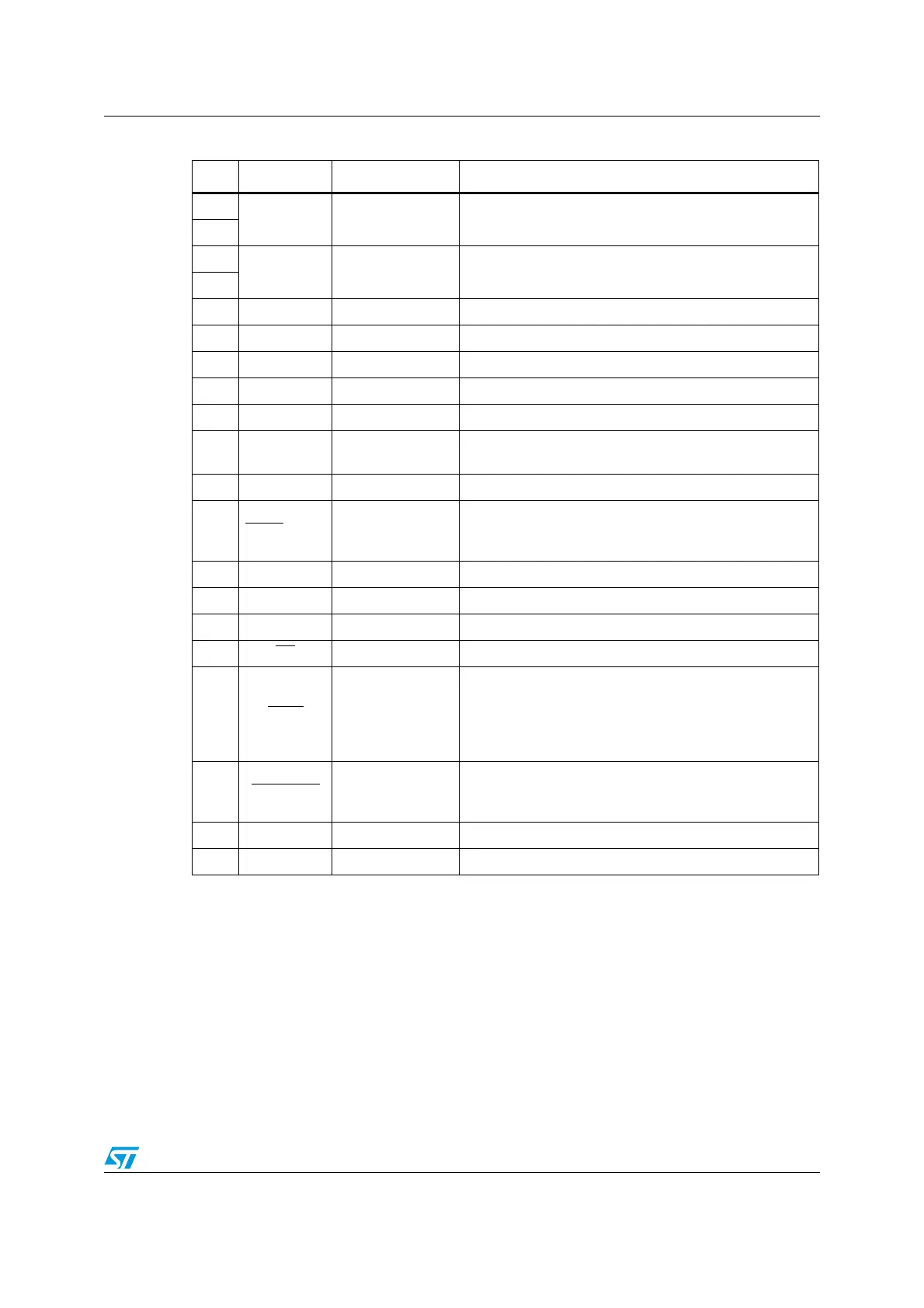
L6470 Pin connection
Doc ID 16737 Rev 2 17/64
12
VSB Power supply
Full bridge B power supply pin. must be connected to
V
SA
16
27
PGND Ground Power ground pin
13
1 OUT1A Power output Full bridge A output 1
28 OUT2A Power output Full bridge A output 2
14 OUT1B Power output Full bridge B output 1
15 OUT2B Power output Full bridge B output 2
9 AGND Ground Analog ground.
4 SW Logical input
External switch input pin. If not used the pin should be
connected to VDD.
21 DGND Ground Digital ground
22 BUSY
\SYNC Open drain output
By default this BUSY pin is forced low when the device is
performing a command. Otherwise the pin can be
configured to generate a synchronization signal.
18 SDO Logic output Data output pin for serial interface
20 SDI Logic input Data input pin for serial interface
19 CK Logic input Serial interface clock
23 CS Logic input Chip Select input pin for serial interface
24 FLAG
Open drain output
Status Flag pin. An internal open drain transistor can pull
the pin to GND when a programmed alarm condition
occurs (step loss, OCD, thermal pre-warning or
shutdown, UVLO, wrong command, non performable
command)
3 STBY\RST
Logic input
Standby and reset pin. LOW logic level reset the logic
and puts the device in standby mode. If not used, should
be connected to VDD
25 STCK Logic input Step clock input
EPAD Exposed pad Ground Internally connected to PGND, AGND and DGND pins
Table 5. Pin description (continued)
N. Name Type Function