Hardware layout and configuration UM2435
24/48 UM2435 Rev 2
Moreover, the board embeds a level shifter, which allows the user to debug the firmware
even if the target (STM32WB55) is supplied by a low-level voltage (1.8 to 3.3 V). There is no
jumper on the USB dongle.
The default jumper configuration and the V
DD
= 1.8 V setting is done according to Table 3.
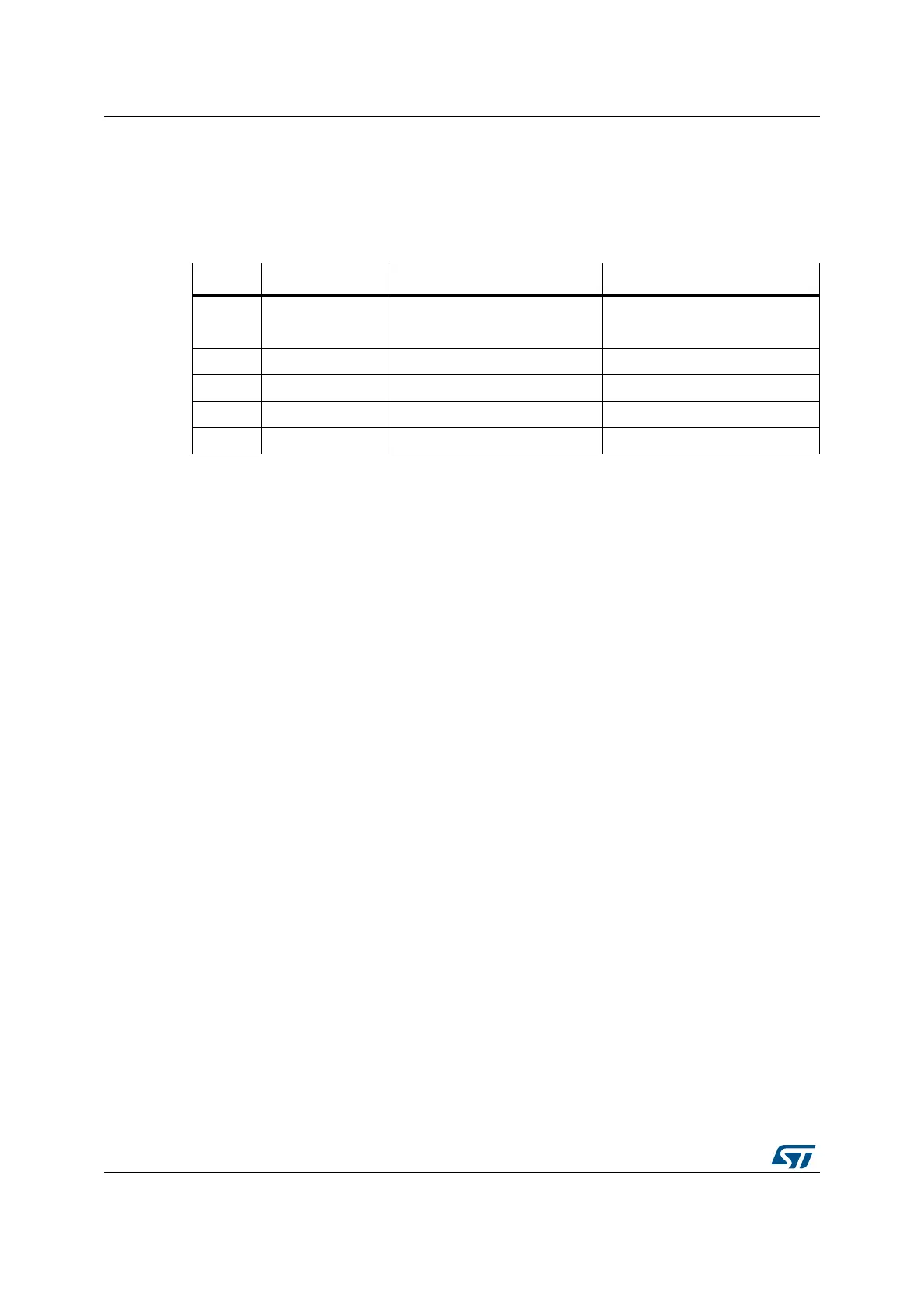
Table 4. Default jumper configuration
Jumper Definition Default position Comment
JP1 Power selection ON [7-8] 5 V from ST-LINK
JP2 I
DD
measurement ON V
DD
current measurement
JP3 I
DD
measurement ON MCU V
DD
current measurement
JP4 RF power ON Possibility of isolating RF power
JP5 Level shifter All ON, except [1-2] that is OFF Level shifter
JP6 VDD_IN_SMPS ON V
DD
SMPS
 Loading...