7 STLINK-V3PWR functional description
7.1 STLINK-V3PWR overview
The following sections provide a functional description of the STLINK-V3PWR features.
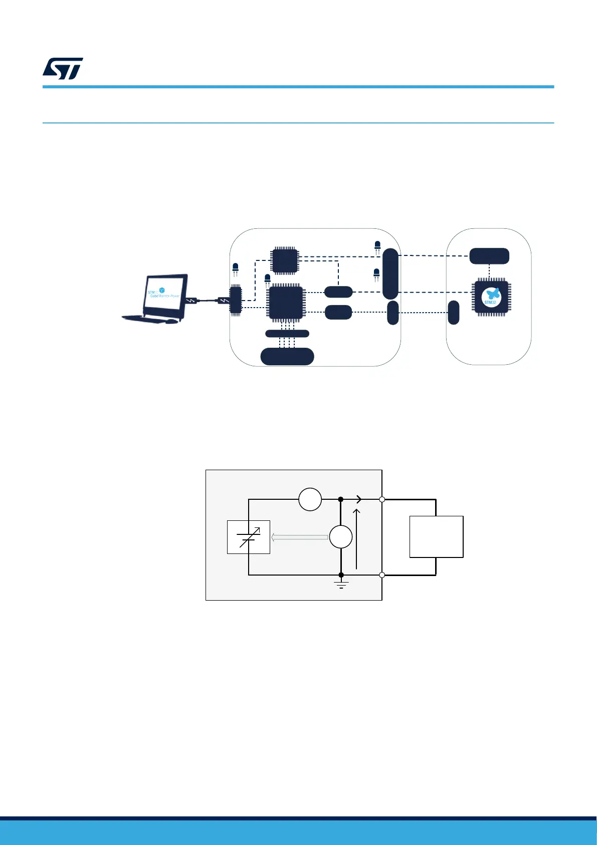
Figure 6 provides a high-level block diagram of the
STLINK-V3PWR internal circuitry that illustrates a typical
connection of STLINK-V3PWR with a host PC and with a target application.
Figure 6. STLINK-V3PWR block diagram
DT59120V1
SMU
USB Type C®
DEBUG
POWER
AUX
OUT
Bridge
USB
COM
OUT
AUX
STLINK-V3PWR
Target
DEBUG
STPMIC1
Level shifter
Level
shifter
Peripherals
STM32H745
VDD
7.2 SMU output (OUT)
The STLINK-V3PWR’s SMU output is accessible on the POWER’s 3‑pin screw connector between the OUT pin
(positive node) and GND pin (negative node). Figure 7 provides a block diagram of the SMU.
Figure 7. STLINK-V3PWR
SMU block diagram
DT59121V1
OUT
V
SOURCE
A
I
meter
V
Feedback to
regulate V
OUT
I
OUT
Target
application
GND
V
OUT
SMU
UM3097
STLINK-V3PWR functional description
UM3097 - Rev 1
page 11/30