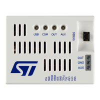
Table 17. DEBUG STDC14
connector pinout
Pin No. Type Description Pin No. Type Description
1 -
NC
(1)
2 - NC
3 I
T_VCC
(2)
4 I/O T_JTMS/T_SWDIO
5 S GND 6 O T_JCLK/T_SWCLK
7 S GND 8 I
T_JTDO/T_SWO
(3)
9 - NC 10 O T_JTDI/NC
11 O
GNDDetect
(4)
12 O T_NRST
13 O T_VCP_RX 14 I T_VCP_TX
1. NC means not connected.
2. Input reference voltage for debug interface level shifters (must be connected into target application onto VDDIO domain)
3. T_SWO: SWO is optional, and required only for Serial Wire Viewer (SWV) trace.
4. Tied to GND by the STLINK-V3PWR firmware after its initialization. Might be used by the target for the detection of the tool.
Note: T_VCC signal on the DEBUG connector is internally connected with the T_VCC signal of the BRIDGE connector
(refer to Section 9.4 BRIDGE (I
2
C, CAN, SPI, UART, and GPIO)).
Note: Debug and bridge interfaces share the same UART interface. T_VCP_RX is internally connected with
UART_TXD of the BRIDGE connector. T_VCP_TX is internally connected with UART_RXD of the BRIDGE
connector (Section 9.4 BRIDGE (I
2
C, CAN, SPI, UART, and GPIO)).
9.4
BRIDGE (I
2
C, CAN, SPI,
UART, and GPIO)
All the bridge functions are provided on a 2x11-pin connector with a 2.54 mm pitch. The related pinout is listed
below:
T
able 18. BRIDGE connector pinout
- Pin name Type Description Features Pin name Type Description Features
Bottom
TGO O TRIG_OUT SMU trigger
Top
TGI I TRIG_IN SMU trigger
IO0 I/O Bridge_GPIO0
GPIO bridge
NSS O SPI_NSS
SPI bridge
IO1 I/O Bridge_GPIO1 MOSI O SPI_MOSI
IO2 I/O Bridge_GPIO2 MISO I SPI_MISO
IO3 I/O Bridge_GPIO3 SCK O SPI_SCK
+5V S
+5V
(1)
- GND S GND -
GND S GND - TVCC I
T_VCC
(2)
-
RTS O UART_RTS
UART
VCP
SCL O I2C_SCL
I
2
C
bridge
RXD I UART_RXD CRX I CAN_RX
CAN bridge
TXD O UART_TXD CTX O CAN_TX
CTS I UART_CTS SDA I/O I2C_SDA
I
2
C
bridge
1.
Supply output (100 mA max) powered from USB-C voltage. Reserved to power supply a daughterboard to be connected
onto the BRIDGE connector.
2. Input reference voltage for bridge interface level shifters (must be connected into target application onto VDDIO domain)
Note: T_VCC signal on the BRIDGE connector is internally connected with the T_VCC signal of the DEBUG connector
(refer to Section 9.3 DEBUG (STM32 JTAG/SWD and VCP)).
Note: Debug and bridge interfaces share the same UART interface. T_VCP_RX is internally connected with
UART_TXD of the BRIDGE connector. T_VCP_TX is internally connected with UART_RXD of the BRIDGE
connector (refer to Section 9.3 DEBUG (STM32 JTAG/SWD and VCP)).
UM3097
BRIDGE (I2C, CAN, SPI, UART, and GPIO)
UM3097 - Rev 1
page 22/30