9 Board connectors description
9.1 Conventions
Per conventions, refer to T
able 15 for the I/O type definition:
Table 15. I/O type definition
Type Definition
I Signal is an input for STLINK-V3PWR and an output for the target application
O Signal is an output for STLINK-V3PWR and an input for the target application
I/O Bidirectional signal or can be configured as input or output (default input)
S Supply pin
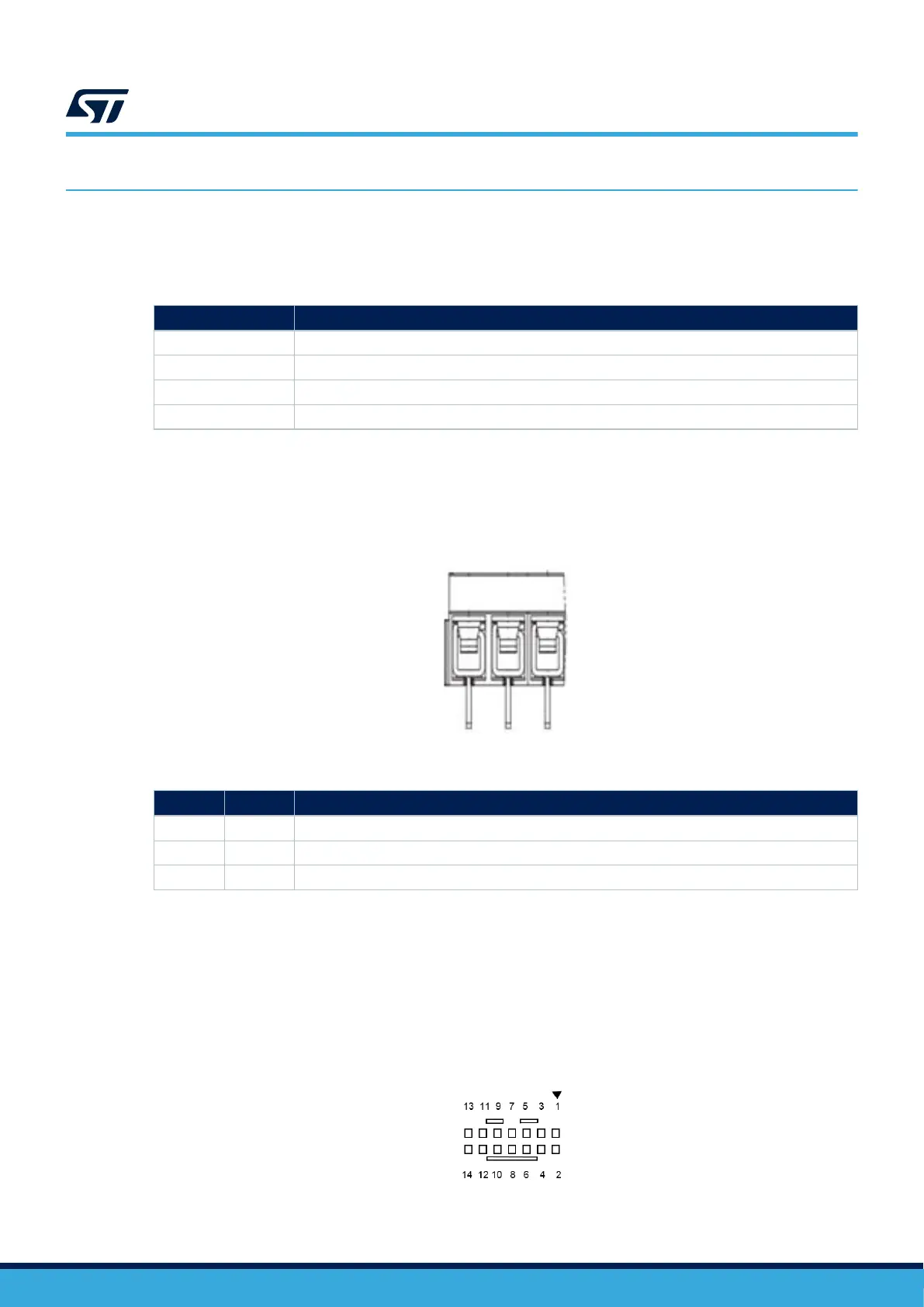
9.2 POWER (OUT/AUX)
The POWER connector (Figure 10) is a 3‑pin screw terminal block with a 5.00 mm pitch. It is used to supply a
target application using cables.
Figure 10. POWER connector (front view)
Table 16. Power connector pinout
Name Type Description
OUT S SMU output (refer to Section 7.2)
GND S Ground
AUX S Auxiliary power source output (refer to Section 7.3)
9.3 DEBUG (STM32 JTAG/SWD and VCP)
The DEBUG (STDC14) connector in Figure 1
1 is a 2x7‑pin with a 1.27 mm pitch. It allows connection to an
STM32 target using the JTAG or SWD protocol, respecting (from pin 3 to pin 12) the MIPI10/ARM10 pinout (Arm
®
Cortex
®
debug connector).
It also provides two UART signals for the Virtual COM port. The related pinout for the DEBUG connector is listed
in Table 17.
Figure 11. DEBUG STDC14 connector (top view)
UM3097
Board connectors description
UM3097 - Rev 1
page 21/30