Hardware layout and configuration UM1974
22/85 UM1974 Rev 9
The 5 V power source is selected by the jumper JP3 as shown in Table 8.
Table 7. External power sources
Input power
name
Connector
pins
Voltage
range
Max current Limitation
V
IN
CN8 pin 15
CN11 pin 24
7 V to 12 V 800 mA
From 7 V to 12 V only and input
current capability is linked to input
voltage:
800 mA input current when V
IN
=7 V
450 mA input current when
7 V<V
IN
<9 V
250 mA input current when
9 V<V
IN
<12 V
E5V CN11 pin 6
4.75 V to
5.25 V
500 mA -
+3.3 V
CN8 pin 7
CN11 pin 16
3 V to 3.6 V -
Two possibilities:
ST-LINK PCB is cut
SB3 and SB111 OFF (ST-LINK not
powered)
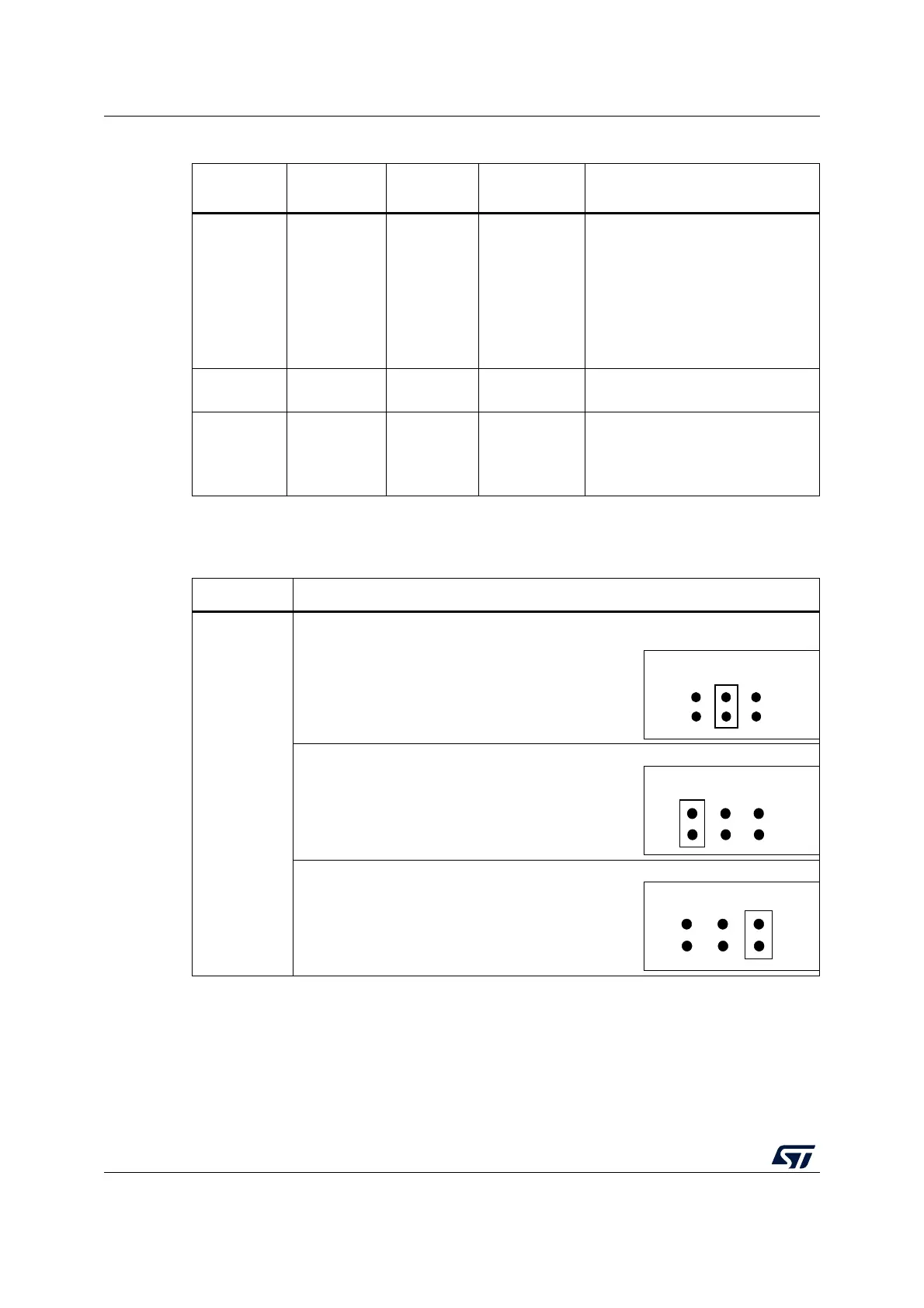
Table 8. Power related jumper
Jumper Description
JP3
U5V (ST-LINK V
BUS
) is used as power source when JP3 is set as shown to the right
(Default setting)
E5V is used as power source when JP3 is set as shown to the right:
V
IN
is used as power source when JP3 is set as shown to the right:
E5V
U5V
VIN-5V
E5V
U5V
VIN-5V