Hardware layout and configuration UM1974
48/85 UM1974 Rev 9
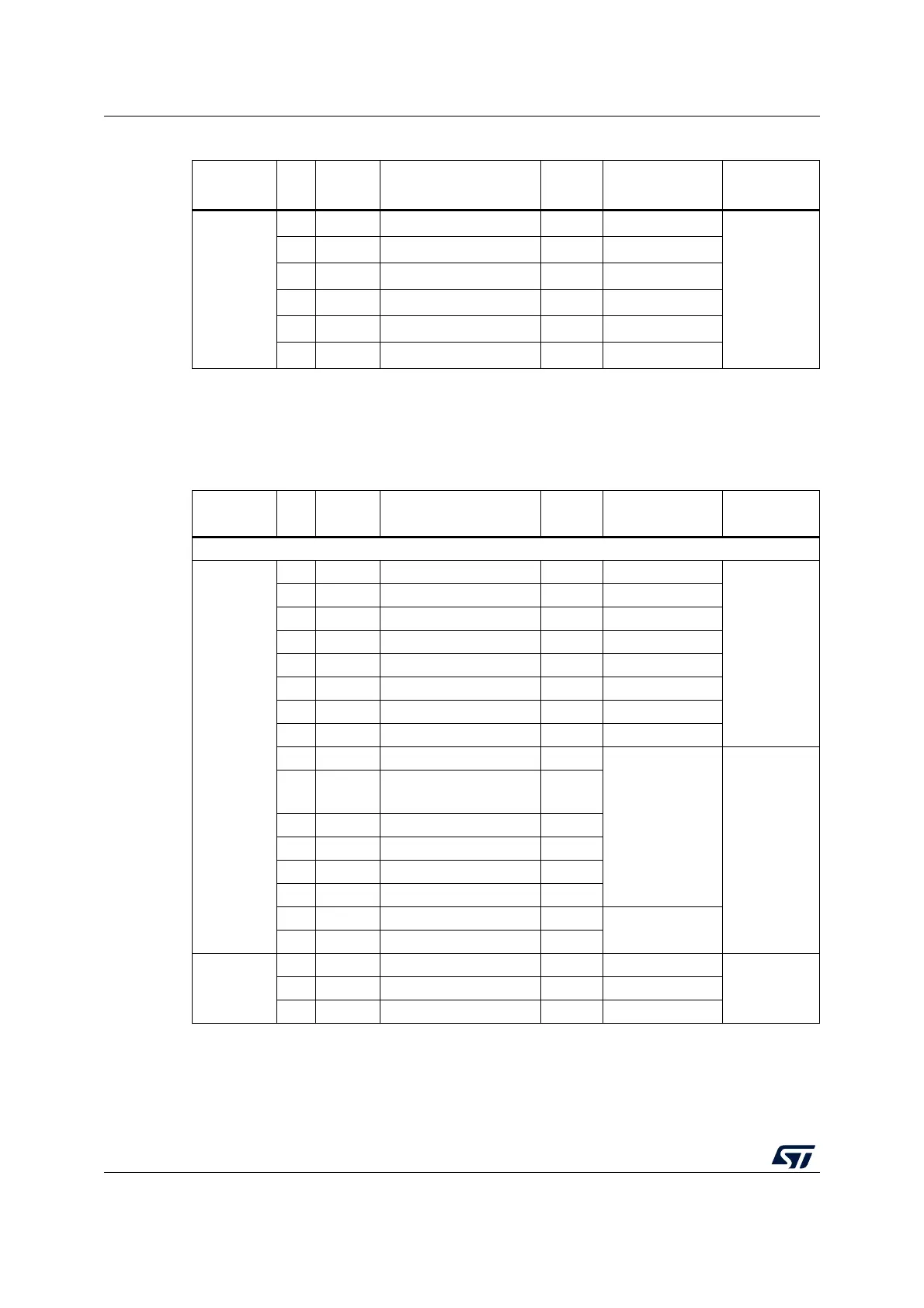
CN10
24 D40 TIMER_A_PWM2N PE10 TIM1_CH2N
-
26 D39 TIMER_A_PWM3N PE12 TIM1_CH3N
28 D38 I/O PE14 I/O
30 D37 TIMER_A_BKIN1 PE15 TIM1_BKIN1
32 D36 TIMER_C_PWM2 PB10 TIM2_CH3
34 D35 TIMER_C_PWM3 PB11 TIM2_CH4
1. For more details refer to Table 12: Solder bridges.
2. PE2 is connected to both CN9 pin 14 (I/O) and CN10 pin 25 (QSPI_BK1_IO2). Only one pin must be used
at one time.
Table 16. NUCLEO-F413ZH pin assignments
Connector Pin
Pin
name
Signal name
STM32
pin
Function Remark
Left connectors
CN8
1NC NC - -
ARDUINO
®
compatible
3 IOREF IOREF - 3.3 V Ref
5 RESET RESET NRST RESET
7 +3.3 V +3.3 V - 3.3 V input/output
9 +5 V +5 V - 5 V output
11 GND GND - ground
13 GND GND - ground
15 V
IN
V
IN
- Power input
2 D43 SDMMC_D0 PC8
SDMMC/I2S_A
-
4D44
SDMMC_D1/
I2S_A_CKIN
PC9
6 D45 SDMMC_D2 PC10
8 D46 SDMMC_D3 PC11
10 D47 SDMMC_CK PC12
12 D48 SDMMC_CMD PD2
14 D49 I/O PG2
I/O
16 D50 I/O PG3
CN9
1 A0 ADC PA3 ADC1_IN3
ARDUINO
®
compatible
3 A1 ADC PC0 ADC1_IN10
5 A2 ADC PC3 ADC1_IN13
Table 15. NUCLEO-F412ZG pin assignments (continued)
Connector Pin
Pin
name
Signal name
STM32
pin
Function Remark