Hardware layout and configuration UM1974
70/85 UM1974 Rev 9
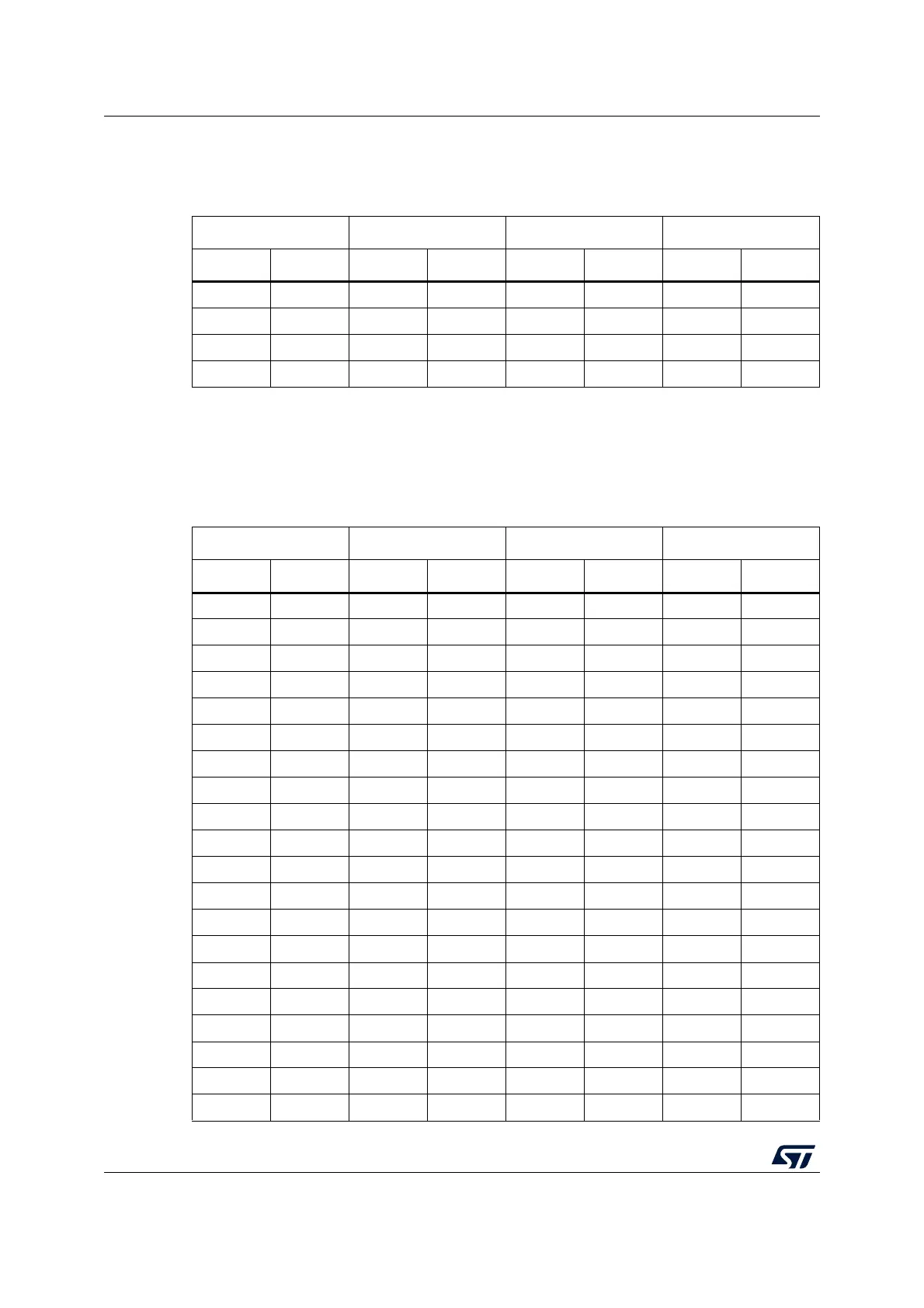
63 PG9 64 PG15 63 GND 64 PE0
65 PG12 66 PG10 65 PD10 66 PG8
67 - 68 PG13 67 PG7 68 PG5
69 PD9 70 PG11 69 PG4 70 PG6
1. Default state of BOOT0 is 0. It can be set to 1 when a jumper is plugged on the pins 5-7 of CN11.
2. U5V is the 5 V power coming from the ST-LINKV2-1 USB connector that rises before and it rises before the
+5 V rising on the board.
3. PA13 and PA14 are shared with SWD signals connected to ST-LINK/V2-1. If ST-LINK part is not cut, it is
not recommended to use them as I/O pins.
Table 22. ST morpho connector for NUCLEO-F303ZE
CN11 odd pins CN11 even pins CN12 odd pins CN12 even pins
Pin Name Pin Name Pin Name Pin Name
1PC102PC111PC92PC8
3 PC12 4 PD2 3 PB8 4 PC6
5 VDD 6 E5V 5 PB9 6 PC5
7BOOT0
(1)
8GND7AVDD8U5V
(2)
9PF610 - 9GND10PD8
11 PF7 12 IOREF 11 PA5 12 PA12
13 PA13
(3)
14 RESET 13 PA6 14 PA11
15 PA14
(3)
16 +3.3 V 15 PA7 16 PB12
17 PA15 18 +5 V 17 PB6 18 PB11
19 GND 20 GND 19 PC7 20 GND
21 PB7 22 GND 21 PA9 22 PB2
23 PC13 24 V
IN
23 PA8 24 PB1
25 PC14 26 - 25 PB10 26 PB15
27 PC15 28 PA0 27 PB4 28 PB14
29 PF0 30 PA1 29 PB5 30 PB13
31 PF1 32 PA4 31 PB3 32 AGND
33 V
BAT
34 PB0 33 PA10 34 PC4
35PC236PC1 35PA236PF5
37PC338PC037PA338PF4
39 PD4 40 PD3 39 GND 40 PE8
Table 21. ST morpho connector for NUCLEO-F207ZG, NUCLEO-F412ZG,
NUCLEO-F413ZH, NUCLEO-F429ZI, NUCLEO-F439ZI, NUCLEO-F446ZE,
NUCLEO-F722ZE, NUCLEO-F746ZG, NUCLEO-F756ZG,
NUCLEO-F767ZI and NUCLEO-H743ZI (continued)
CN11 odd pins CN11 even pins CN12 odd pins CN12 even pins
Pin Pin name Pin Pin name Pin Pin name Pin Pin name