UM1974 Rev 9 71/85
UM1974 Hardware layout and configuration
84
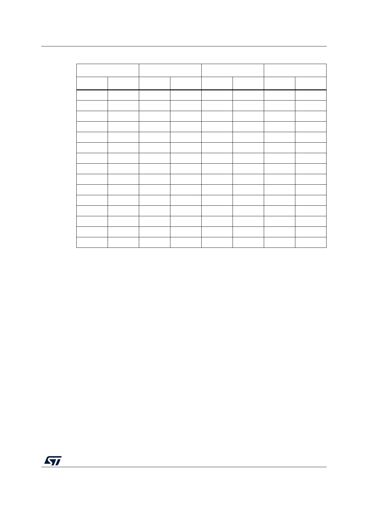
41 PD5 42 PG2 41 PD13 42 PF10
43 PD6 44 PG3 43 PD12 44 PE7
45 PD7 46 PE2 45 PD11 46 PD14
47 PE3 48 PE4 47 PE10 48 PD15
49 GND 50 PE5 49 PE12 50 PF14
51 PH1 52 PF2 51 PE14 52 PE9
53 PH0 54 PF8 53 PE15 54 GND
55 PD1 56 PF9 55 PE13 56 PE11
57 PD0 58 PG1 57 PF13 58 PF3
59 PG0 60 GND 59 PF12 60 PF15
61 PE1 62 PE6 61 PG14 62 PF11
63 PG9 64 PG15 63 GND 64 PE0
65 PG12 66 PG10 65 PD10 66 PG8
67 PH2 68 PG13 67 PG7 68 PG5
69 PD9 70 PG11 69 PG4 70 PG6
1. Default state of BOOT0 is 0. It can be set to 1 when a jumper is plugged on the pins 5-7 of CN11.
2. U5V is the 5 V power coming from the ST-LINK/V2-1 USB connector that rises before and it rises before
the +5 V rising on the board.
3. PA13 and PA14 are shared with the SWD signals connected to ST-LINK/V2-1. If ST-LINK part is not cut, it
is not recommended to use them as I/O pins.
Table 22. ST morpho connector for NUCLEO-F303ZE (continued)
CN11 odd pins CN11 even pins CN12 odd pins CN12 even pins
Pin Name Pin Name Pin Name Pin Name