Hardware layout and configuration UM1974
44/85 UM1974 Rev 9
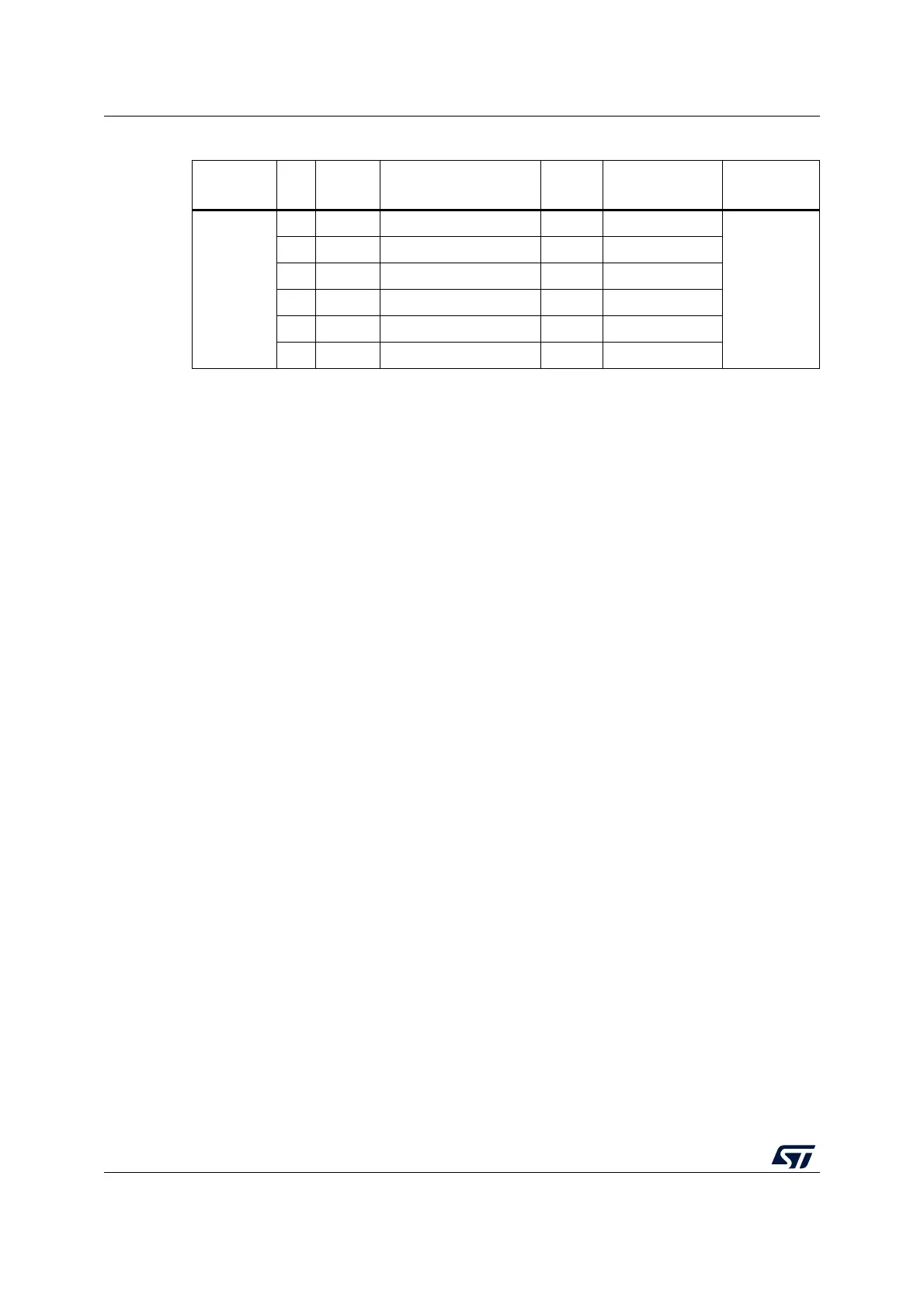
CN10
24 D40 TIMER_A_PWM2N PE10 TIM1_CH2N
-
26 D39 TIMER_A_PWM3N PE12 TIM1_CH3N
28 D38 TIMER_A_BKIN2 PE14 TIM1_BKIN2
30 D37 TIMER_A_BKIN1 PE15 TIM1_BKIN1
32 D36 TIMER_C_PWM2 PB10 TIM2_CH3
34 D35 TIMER_C_PWM3 PB11 TIM2_CH4
1. For more details refer to Table 12: Solder bridges.
2. PA7 is used as D11 and connected to CN7 pin 14 by default, if JP6 is ON, it is also connected to CN9 pin
15 as COMP2_INP. In this case only one function of the Comparator input or D11 must be used.
3. PE2 is connected to both CN9 pin 14 (I/O) and CN10 pin 25 (I/O). Only one connector pin must be used at
one time.
Table 14. NUCLEO-F303ZE pin assignments (continued)
Connector Pin
Pin
name
Signal name
STM32
pin
Function Remark