UM1974 Rev 9 51/85
UM1974 Hardware layout and configuration
84
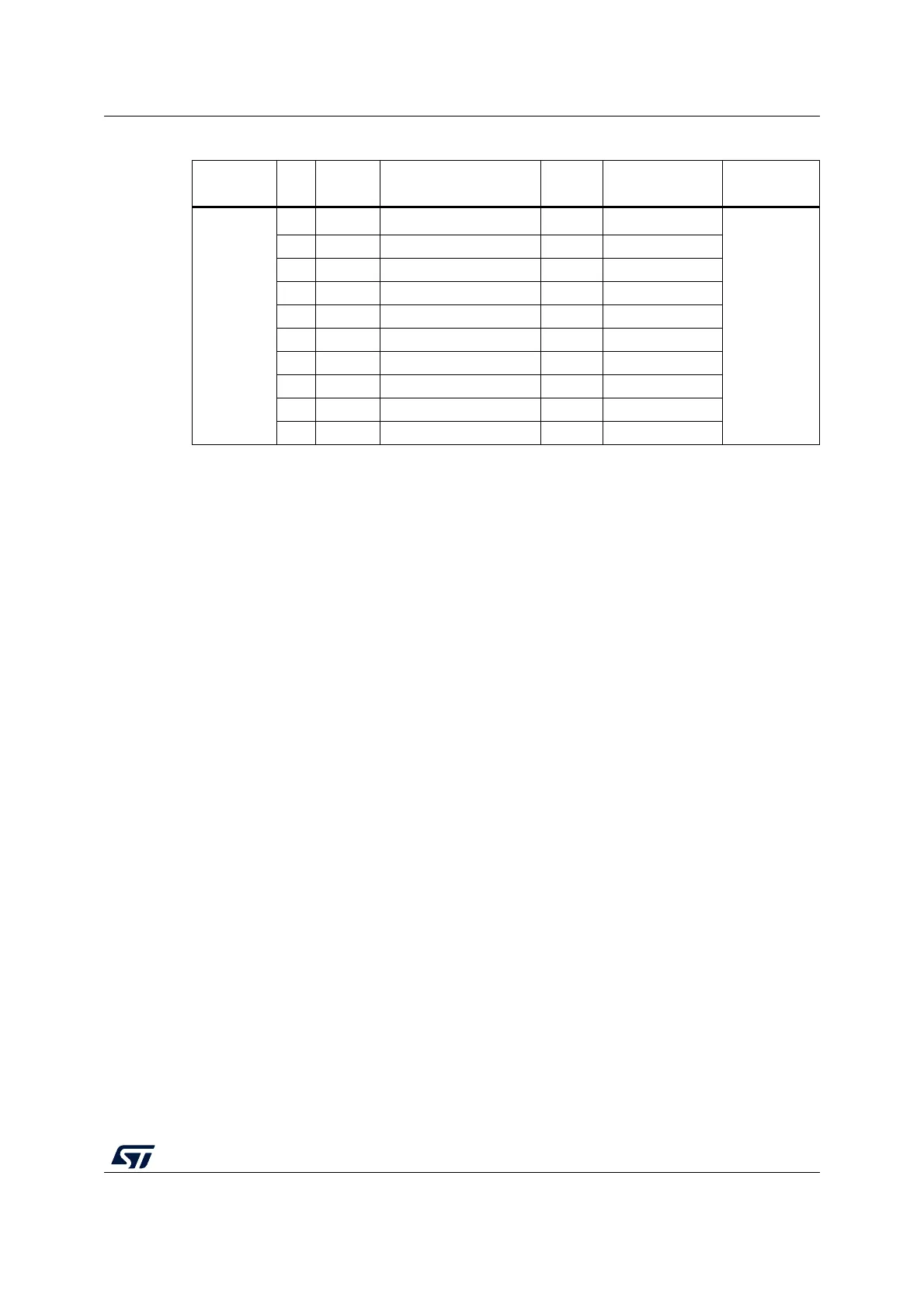
CN10
16 D0 USART_A_RX PG9
ARDUINO
®
compatible
18 D42 TIMER_A_PWM1N PE8 TIM1_CH1N
20 D41 TIMER_A_ETR PE7 TIM1_ETR
22 GND GND - ground
24 D40 TIMER_A_PWM2N PE10 TIM1_CH2N
26 D39 TIMER_A_PWM3N PE12 TIM1_CH3N
28 D38 I/O PE14 I/O
30 D37 TIMER_A_BKIN1 PE15 TIM1_BKIN1
32 D36 TIMER_C_PWM2 PB10 TIM2_CH3
34 D35 TIMER_C_PWM3 PB11 TIM2_CH4
1. For more details refer to Table 12: Solder bridges.
2. PE2 is connected to both CN9 pin14 (SAI_A_MCLK) and CN10 pin25 (QSPI_BK1_IO2). Only one
connector pin can be used at one time.
3. Limitation: SAI_A_SD (PE4) is swapped with SAI_A_FS (PE6). These two pins on CN10 of NUCLEO-
F413ZH are not compatible with other STM32 Nucleo-144 boards.
Table 16. NUCLEO-F413ZH pin assignments (continued)
Connector Pin
Pin
name
Signal name
STM32
pin
Function Remark