2 Device development process
STM32 series product development process (see Figure 1), compliant with the IATF 16949 standard, is a set of
interrelated activities dedicated to transform customer specification and market or industry domain requirements
into a semiconductor device and all its associated elements (package, module, sub-system, hardware, software,
and documentation), qualified with ST internal procedures and fitting ST internal or subcontracted manufacturing
technologies.
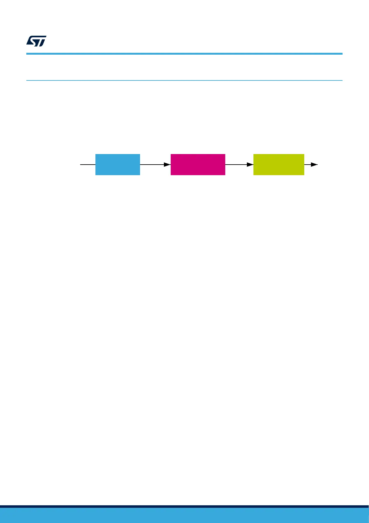
Figure 1. STMicroelectronics product development process
·Key characteristics and
requirements related to future
uses of the device
·Industry domain(s), specific
customer requirements and
definition of controls and tests
needed for compliance
·Product target specification
and strategy
·Project manager
appointment to drive product
development
·Evaluation of the
technologies, design tools
and IPs to be used
·Design objective
specification and product
validation strategy
·Design for quality
techniques (DFD, DFT, DFR,
DFM, …) definition
·Architecture and positioning
to make sure the software
and hardware system
solutions meet the target
specification
·Product approval strategy
and project plan
·Semiconductor design
development
·Hardware development
·Software development
·Analysis of new product
specification to forecast
reliability performance
·Reliability plan, reliability
design rules, prediction of
failure rates for operating life
test using Arrhenius’s law and
other applicable models
·Use of tools and
methodologies such as
APQP, DFM, DFT, DFMEA
·Detection of potential
reliability issues and solution
to overcome them
·Assessment of Engineering
Samples (ES) to identify the
main potential failure
mechanisms
·Statistical analysis of
electrical parameter drifts for
early warning in case of fast
parametric degradation (such
as retention tests)
·Failure analysis on failed
parts to clarify failure modes
and mechanisms and identify
the root causes
·Physical destructive
analysis on good parts after
reliability tests when required
·Electrostatic discharge
(ESD) and latch-up sensitivity
measurement
·Successful completion of
the product qualification
plan
·Secure product deliveries
on advanced technologies
using stress methodologies
to detect potential weak
parts
·Successful completion of
electrical characterization
·Global evaluation of new
product performance to
guarantee reliability of
customer manufacturing
process and final application
of use (mission profile)
·Final disposition for
product test, control and
monitoring
1 Conception
3 Qualification
2 Design and
validation
UM2305
Device development process
UM2305 - Rev 10
page 4/110

 Loading...


