3-71
Figure 3-9. Vertical Vector Generator.
_____ __.J
DI SPLA Y CON T RO L
NEil POSITION STEP
VOLTAGE FROM INP U T
BUF F ER U1 7 0
4917- 10
R160
12
VERT -5
R161
VE CTOR '? R141 R 192 ~
U27 0B
AC
CO MP
t
~ _ll
c:::
SAM P L E
PEAKI N G
'~
~
SIiITCH
R276 +5 C9 2 5~~
~+
R605 ~
R172 U28 1
"-
I :1 "~C9 15
~
~.
~
R6 20
V
~
I
C260 "R 27 3
:(l
U28 0
u
R162
~r-
INTE G
R6 03 CJf0
C281 ADJ
II
R60 1 C180
R280
HOLD
R2 74
)f-
I
CAPACITO R
HI GH- CUR RE NT DI FFE RENCE AM PL
I
I
SAMPLE- A ND -H OL D
INTEG RA TOR
--
I
SAMP L E FRO M
OLD PO SITION VO LTA GE
VE CTORS TO
MODE SE LE C T
SIIITC H U2 90B
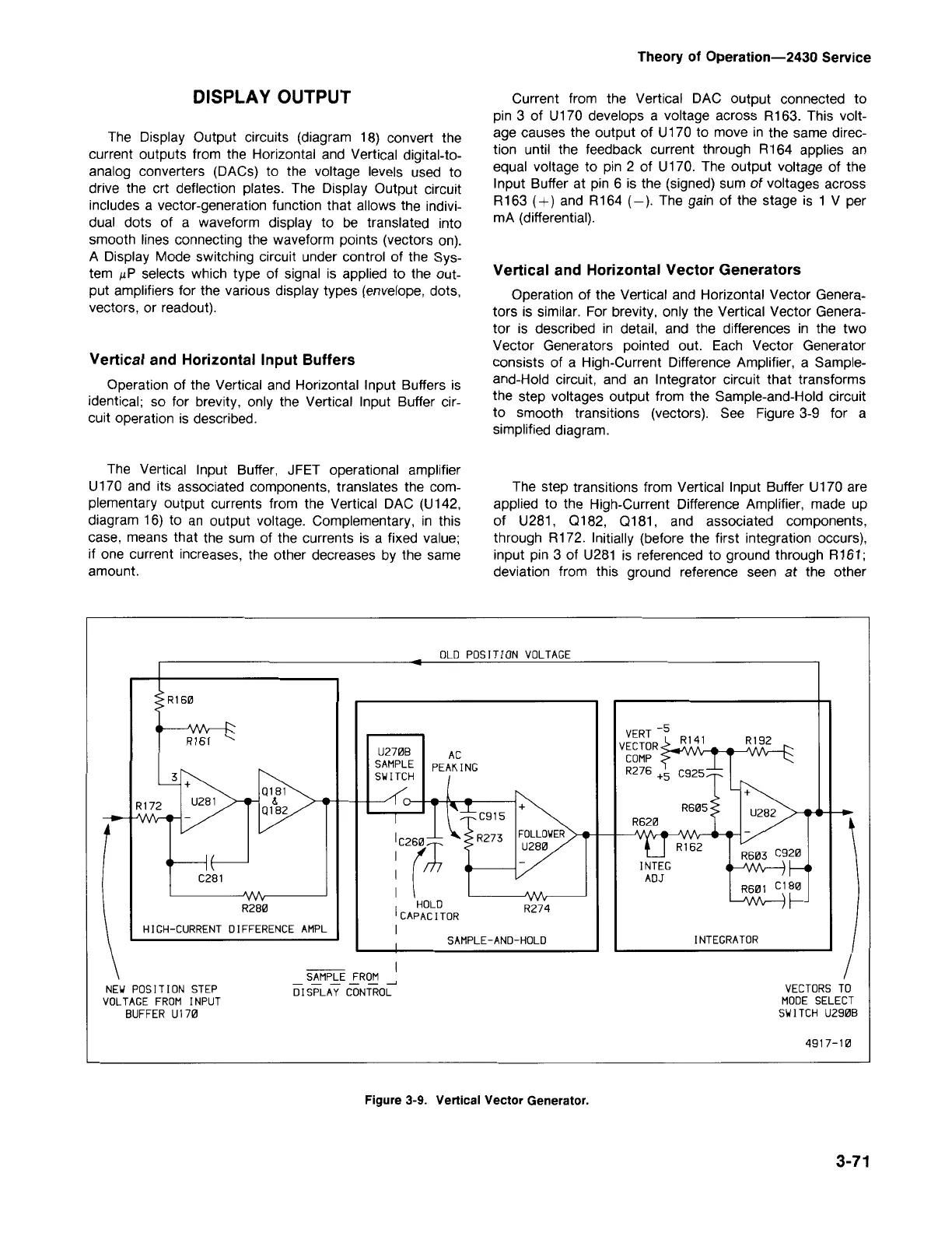
The step transitions from Vertical Input Buffer U170 are
applied to the High-Current Difference Amplifier, made up
of U281, Q182, Q181, and associated components,
through R172. Initially (before the first integration occurs),
input pin 3 of U281 is referenced to ground through R161;
deviation from this ground reference seen at the other
Vertical and Horizontal Vector Generators
Operation of the Vertical and Horizontal Vector Genera-
tors is similar. For brevity, only the Vertical Vector Genera-
tor is described in detail, and the differences in the two
Vector Generators pointed out. Each Vector Generator
consists of a High-Current Difference Amplifier, a Sample-
and-Hold circuit, and an Integrator circuit that transforms
the step voltages output from the Sample-and-Hold circuit
to smooth transitions (vectors). See Figure 3-9 for a
simplified diagram.
Current from the Vertical DAC output connected to
pin 3 of U170 develops a voltage across R163. This volt-
age causes the output of U170 to move in the same direc-
tion until the feedback current through R164 applies an
equal voltage to pin 2 of U170. The output voltage of the
Input Buffer at pin 6 is the (signed) sum of voltages across
R163
(+)
and R164 (-). The gain of the stage is 1 V per
mA (differential).
Theory of Operation-2430 Service
The Vertical Input Buffer, JFET operational amplifier
U170 and its associated components, translates the com-
plementary output currents from the Vertical DAC (U142,
diagram 16) to an output voltage. Complementary, in this
case, means that the sum of the currents is a fixed value;
if one current increases, the other decreases by the same
amount.
Vertical and Horizontal Input Buffers
Operation of the Vertical and Horizontal Input Buffers is
identical; so for brevity, only the Vertical Input Buffer cir-
cuit operation is described.
The Display Output circuits (diagram 18) convert the
current outputs from the Horizontal and Vertical digital-to-
analog converters (DACs) to the voltage levels used to
drive the crt deflection plates. The Display Output circuit
includes a vector-generation function that allows the indivi-
dual dots of a waveform display to
be
translated into
smooth lines connecting the waveform points (vectors on).
A Display Mode switching circuit under control of the Sys-
tem !-,p selects which type of signal is applied to the out-
put amplifiers for the various display types (envelope, dots,
vectors, or readout).
DISPLA Y OUTPUT

 Loading...


