3-19
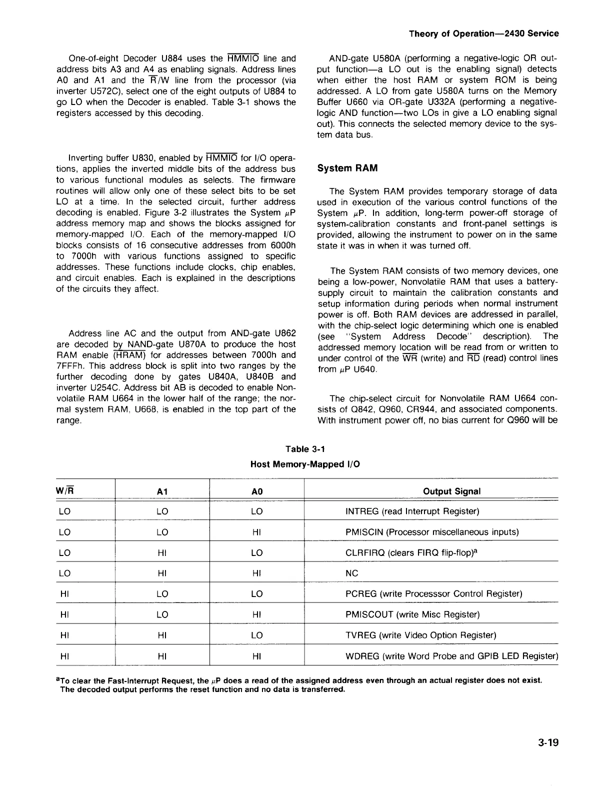
aTo clear the Fast-Interrupt Request,theI1Pdoes a read of the assigned address even through an actual register does not exist.
The decoded output performs the reset function and no data is transferred.
wi"R
A1 AO
Output Signal
LO LO LO
INTREG (read Interrupt Register)
LO LO HI
PMISCIN (Processor miscellaneous inputs)
LO HI LO
CLRFIRO (clears FIRO flip-flop)a
LO HI HI NC
HI LO LO
PCREG (write Processsor Control Register)
HI LO HI
PMISCOUT (write Misc Register)
HI
HI
LO
TVREG (write Video Option Register)
HI HI HI
WDREG (write Word Probe and GPIB LED Register)
Table 3-1
Host Memory-Mapped I/O
The chip-select circuit for Nonvolatile RAM U664 con-
sists of
0842, 0960,
CR944, and associated components.
With instrument power off, no bias current for 0960 will be
The System RAM consists of two memory devices, one
being a low-power, Nonvolatile RAM that uses a battery-
supply circuit to maintain the calibration constants and
setup information during periods when normal instrument
power is off. Both RAM devices are addressed in parallel,
with the chip-select logic determining which one is enabled
(see "System Address Decode" description). The
addressed memory location will be read from or written to
under control of the WR (write) and RD (read) control lines
from /-lPU640.
The System RAM provides temporary storage of data
used in execution of the various control functions of the
System /-lP. In addition, long-term power-off storage of
system-calibration constants and front-panel settings is
provided, allowing the instrument to power on in the same
state it was in when it was turned off.
System
RAM
AND-gate U580A (performing a negative-logic OR out-
put function-a LO out is the enabling signal) detects
when either the host RAM or system ROM is being
addressed. A LO from gate U580A turns on the Memory
Buffer U660 via OR-gate U332A (performing a negative-
logic AND function-two LOs in give a LO enabling signal
out). This connects the selected memory device to the sys-
tem data bus.
Theory of Operation-2430 Service
Address line AC and the output from AND-gate U862
are decoded by NAND-gate U870A to produce the host
RAM enable (HRAM) for addresses between 7000h and
7FFFh. This address block is split into two ranges by the
further decoding done by gates U840A, U840B and
inverter U254C. Address bit AB is decoded to enable Non-
volatile RAM U664 in the lower half of the range; the nor-
mal system RAM, U668, is enabled in the top part of the
range.
Inverting buffer U830, enabled by HMMIO for I/O opera-
tions, applies the inverted middle bits of the address bus
to various functional modules as selects. The firmware
routines will allow only one of these select bits to be set
LO at a time. In the selected circuit, further address
decoding is enabled. Figure 3-2 illustrates the System ,uP
address memory map and shows the blocks assigned for
memory-mapped I/O. Each of the memory-mapped I/O
blocks consists of 16 consecutive addresses from 6000h
to 7000h with various functions assigned to specific
addresses. These functions include clocks, chip enables,
and circuit enables. Each is explained in the descriptions
of the circuits they affect.
One-of-eight Decoder U884 uses the HMMIO line and
address bits A3 and A4 as enabling signals. Address lines
AO and A 1 and the
R
/W line from the processor (via
inverter U572C), select one of the eight outputs of U884 to
go LO when the Decoder is enabled. Table 3-1 shows the
registers accessed by this decoding.