REVJUL 1987
When 16 sampleshave been acquired in the A register,
the TI (transferinto B) clock moves all 16 samples from
the
.p
1A cells in parallel into the B register. The four
phases of the B clocks shift samples down the 16 parallel
B registers in a manner similar to that just described for
the A register but at 1/16th the rate. The TTL1B clock
(TTL-version of B clock
.p
1) is output to the Time Base
Controller and allows it to keep track of how many sam-
ples have been acquired(in multiples of 32). This allows
the Time Base Controller to know when the proper
number of "pretrigger" points have been acquired and
when to enablethe Trigger LogicArray.
Depending on whether the Side 1 channel or Side3
channel is being acquired,the correspondingsample gate
(SAM1 or SAM3) will go HI. This movesthe present level
of the input signalinto the input well of the CCO arrays.
Before the sample gate returns LO, the
.p
1A (phase 1-A
register) clock goes HI and the charge is shared by the
adjacent cells (input and
.p
1). When the sample gate
returns LO, all charge movesto the
.p 1
cell. The.p2Aclock
then goes HI and charge is distributed into both the
.p
1
and
.p 2
cells. When
.p 1
returns LO, all charge will move
into the
.p 2
cell. Similarshifts occur using the.p3Aand.p4A
clocks until
.p 1
occurs again,completingthe cycle.
FISO MODE.As explainedin the CCOdescription,each
CCO is made up of two identicaldifferentialchannelsusing
a serial-parallel-serial(SPS) structure. Samplesare moved
into and shifted within the CCO arrays using properly
phased,overlappingclocks. Figure3-5 shows a basic CCO
structure (seeCCD description,diagram 10).
Two operating modes exist for the CCO arrays; FISO
(fast-in, slow-out) and Short-Pipe.The Phase Clock circuit
is set up to generate proper clocking signals for either
mode by loading data into Gate Array Control Register
U270 (diagram5). This data is applied to U470 on the
CCO-CC3(chip control 0-3) lines and on the POOFF(peak
detector Off) line. The POOFFline enables/disables the
peak-detector output lines (P01, P01, P02, and P02) and
thus peak detection mode (see that description). The
CCO-CC3inputs control operating mode and clock selec-
tion as shown in Table3-7.
The CCD Phase Clock generates properly phased and
frequency-relatedclocks that control most of the Acquisi-
tion system. These functionsinclude moving samples into
the CCOarrays, shifting within the arrays, jitter-correction
control, peak-detection control, and trigger-delay clock
generation. These clocks are derived from the 200/250
MHz master clock generatedby the internal oscillator and
the PhaseLocked Loop circuit.
CCO Phase Clock
3-52
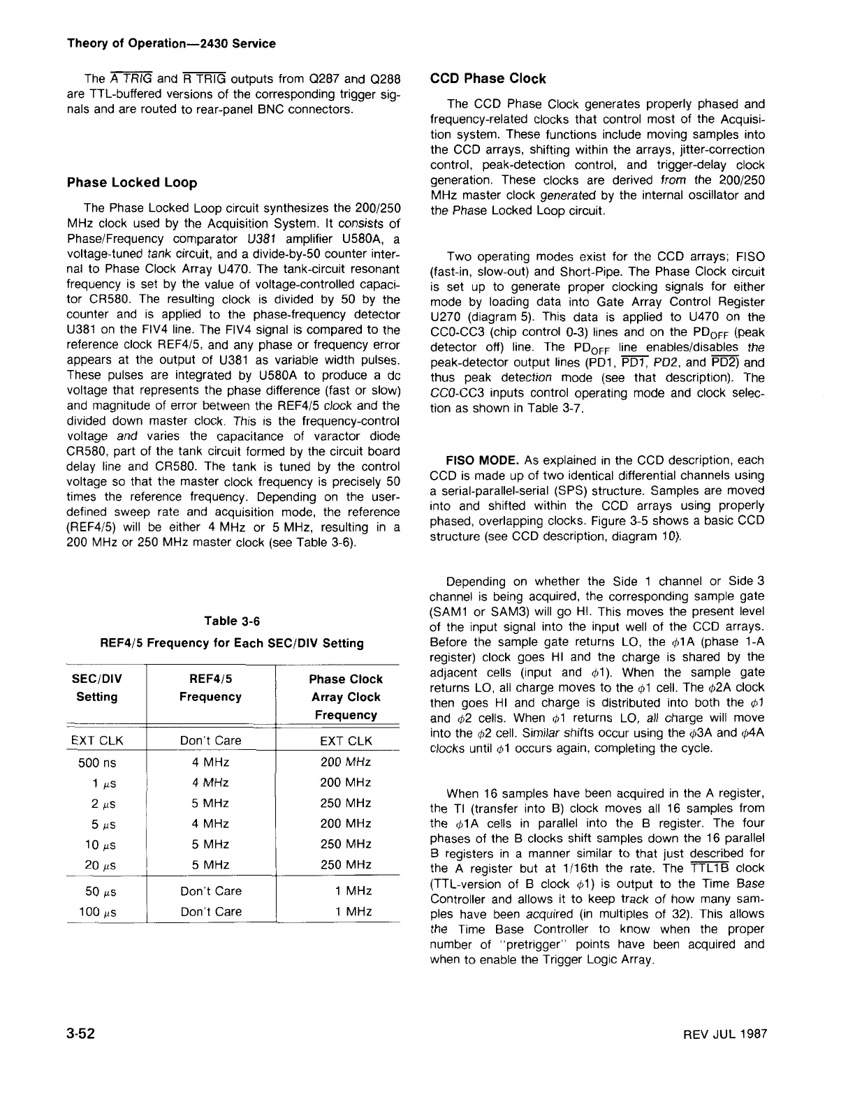
SEC/DIV
REF4/5 Phase Clock
Setting
Frequency
Array Clock
Frequency
EXTCLK
Don't Care
EXTCLK
500 ns
4 MHz
200 MHz
1
ILS
4 MHz
200 MHz
2
ILS
5 MHz
250 MHz
5
ILS
4 MHz 200 MHz
10
ILS
5 MHz
250 MHz
20
ILS
5 MHz
250 MHz
50
ILS
Don't Care
1 MHz
100
ILS
Don't Care
1 MHz
Table 3-6
REF4/5Frequency for Each SEC/DIVSetting
Phase Locked Loop
The PhaseLocked Loop circuit synthesizesthe 200/250
MHz clock used by the Acquisition System. It consists of
Phase/Frequencycomparator U381 amplifier U580A, a
voltage-tunedtank circuit, and a divide-by-50counter inter-
nal to PhaseClock Array U470. The tank-circuit resonant
frequencyis set by the value of voltage-controlledcapaci-
tor CR580. The resulting clock is divided by 50 by the
counter and is applied to the phase-frequencydetector
U381 on the FIV4 line.The FIV4 signal is comparedto the
referenceclock REF4/5,and any phase or frequencyerror
appears at the output of U381 as variable width pulses.
These pulses are integrated by U580A to produce a dc
voltage that representsthe phase difference(fast or slow)
and magnitudeof error between the REF4/5clock and the
divided down master clock. This is the frequency-control
voltage and varies the capacitance of varactor diode
CR580,part of the tank circuit formed by the circuit board
delay line and CR580. The tank is tuned by the control
voltage so that the master clock frequency is precisely50
times the reference frequency. Depending on the user-
defined sweep rate and acquisition mode, the reference
(REF4/5) will be either 4 MHz or 5 MHz, resulting in a
200 MHz or 250 MHz master clock (seeTable3-6).
The A TRIG and R TRIG outputs from 0287 and 0288
are TTL-buffered versions of the corresponding trigger sig-
nals and arerouted to rear-panel BNC connectors.
Theory of Operation-2430 Service